Bipolar Junction transistor
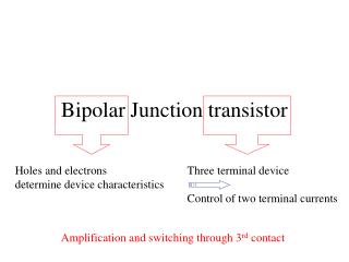
Holes and electrons determine device characteristics. Three terminal device Control of two terminal currents. Bipolar Junction transistor. Amplification and switching through 3 rd contact. V. I. p. n. I. V. I 0. How can we make a BJT from a pn diode?.

Bipolar Junction transistor
E N D
Presentation Transcript
Holes and electrons determine device characteristics Three terminal device Control of two terminal currents Bipolar Junction transistor Amplification and switching through 3rd contact
V I p n I V I0 How can we make a BJT from a pn diode? • Remember reverse bias characteristics • Take pn diode • Reverse saturation current: I0
Test: Multiple choice Why is the reverse bias current of a pn diode small? • Because the bias across the depletion region is small. • Because the current consist of minority carriers injected across the depletion region. • Because all the carriers recombine.
Test: Multiple choice Why is the reverse bias current of a pn diode small? • Because the bias across the depletion region is small. • Because the current consist of minority carriers injected across the depletion region. • Because all the carriers recombine.
V I e- p n h+ • np and pn low • I0 small I V I0 How can we make a BJT from a pn diode? • Remember reverse bias characteristics • Take pn diode • Reverse saturation current: I0 • Caused by minority carriers swept across the junction
V I e- p n h+ I np and/or pn V I0 Test: Multiple choice • If minority carrier concentration can be increased what will happen to I0? • Increase • Decrease • Remain the same
np and pn V I e- p n h+ • If np and pn higher • |I0| larger I V I0 • If minority carrier concentration can be increased near the depletion region edge, then I0 will increase.
V I e- p n h+ I V I0 Test: True-False pn If we only increase then |I0| will still increase.
V I h+ p n e- How can we increase the minority carrier concentration near the depletion region edge? • Take pn diode • Remember forward bias characteristics • How can we make a hole injector from a pn diode? • By increasing the applied bias, V. • By increasing the doping in the p region only • By applying a reverse bias.
V I h+ p n • When using a p+n junction • diode current If ≈ hole current e- I • Ip pno (eeV/kT-1) • In npo (eeV/kT-1) • Since NA >> ND • np << pn • → Ip >> In V If Hole injector • Take pn diode • Remember forward bias characteristics p+
V V I0 I h+ p+ n e- n p e- h+ If W large, then? W Thus: A forward biased p+n diode is a good hole injector A reverse biased np diode is a good minority carrier collector • Recombination of excess holes will occur and excess will be 0 at end of layer • Recombination of excess holes will occur and excess will be large at end of layer • No recombination of excess holes will occur. • Recombination of excess electrons will occur and excess will be np0 at end of layer
V V I I0 dpn h+ p+ n e- n p e- x h+ Lp If W large → holes recombine W Thus: A forward biased p+n diode is a good hole injector A reverse biased np diode is a good minority carrier collector Excess hole concentration reduces exponentially in W to some small value.
V V I I0 dpn h+ p+ n e- n p e- x h+ Lp W What is the magnitude of the hole diffusion current at the edge x=W of the “green” region? • Magnitude of hole diffusion current at x=W is same as at x=0 • Magnitude of hole diffusion current at x=W is almost 0 • Magnitude of hole diffusion current cannot be derived from this layer.
V V I I0 dpn h+ p+ n e- n p e- x h+ Lp if W large → holes recombine W Reduce W Thus: A forward biased p+n diode is a good hole injector A reverse biased np diode is a good minority carrier collector Since gradient of dpn @ x=W is zero, hole diffusion current is also zero
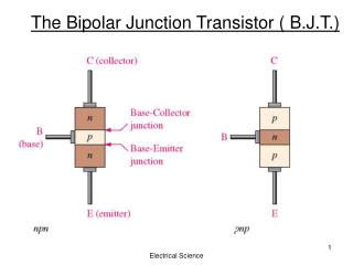
p+ n IC B V V IE I I p VBC W < Lp BJT p+np E: emitter VBC EB B: base E C C: collector C E Common base configuration
Base: Short layer with recombination and no Ohmic contacts at edges. Single junction pno pno npo npo Double junction npo npo pno No Ohmic contact thus minority carrier concentration not
How will we calculate the minority carrier concentration in the base? Rate equation Steady state General solution of second order differential equation With Ohmic contact C1=0 C2≠0 Without Ohmic contact C1≠0 C2≠0
n+-well for emitter p-well for base p+ Si Ohmic contact n+ Si ohmic contact device insulation p-substrate n-well for collector B C E n+ Si p+ Si p+ Si p Si n Si p Si Planar BJT - npn For integrated circuits (ICs) all contacts have to be on the top
E B C IE IC p+ n p holes e- gain, reverse bias holes IE IC ICB0 I’B I”B Recombination e- loss e- loss, forward bias IB Carrier flow in BJTs IB IB = I’B + I”B – ICB0
Electrostatically neutral h+ e- tp recombine with Wb << Lp Control by base current : ideal case. Based upon space charge neutrality Base region IE = Ip tt transit time tt < tp Based on the given timescales, holes can pass through the narrow base before a supplied electron recombines with one hole: ic/ib = tp/tt The electron supply from the base contact controls the forward bias to ensure charge neutrality!
E IC IEp B equilibrium Injection of carriers e- VBE>0 Wb < Lp x h+ No amplification! IEn Amplification! How good is the transistor? C • IEp>>IEn • Wish list: or g = IEp/(IEn + IEp) ≈ 1 g: emitter injection efficiency • IC≈ IEp or B= IC/IEp≈ 1 B: base transport factor or a= IC/IE≈ 1 a: current transfer ratio + (1-B) IEp • IB≈IEn thus b= IC/IB= a/(1-a) b: current amplification factor ICB0 ignored
Forward biased p+n junction is a hole injector Reverse biased np junction is a hole collector B E W < Lp Review 1 – BJT basics IC Forward active mode (ON) IE VBC V V VBC I I EB E C p+ n p C E
Forward biased p+n junction is a hole injector Reverse biased np junction is a hole collector B E W < Lp Review 1 – BJT basics IC Forward active mode (ON) IE VBC V V VBC IB=I’B +I”B I I EB E C p+ n p C E
IB = I’B + I”B – ICB0 Review 2 Amplification? Recombination only case: I’B, ICB0negligible ic/ib = tp/tt Carriers supplied by the base current stay much longer in the base: tp than the carriers supplied by the emitter and travelling through the base: tt. b = tp/tt But in more realistic case: I’Bis not negligible b = IC/IB With IB electrons supplied by base = I’B = In IC holes collected by the collector = Ip
Currents? • In order to calculate currents in pn junctions, knowledge of the variation of the minority carrier concentration is required in each layer. • The current flowing through the base will be determined by the excess carrier distribution in the base region. • Simple to calculate when the short diode approximation is used: this means linear variations of the minority carrier distributions in all regions of the transistor. (recombination neglected) • Complex when recombination in the base is also taken into account: then exponential based minority carrier concentration in base.
E B C p(x) B DpE Without recombination pn0 With recombination pn0 DpC x 0 Wb Minority carrier distribution • Emitter injects majority carriers into base. • dpn(0)=pno (exp(VEB/VT)-1) • Assume active mode: VEB>0 & VBC<0 • Collector collects minority carriers from base. • dpn(Wb)=pno (exp(VBC/VT)-1) dp(x) 0
dp(x) B DpE DpC x 0 Wb See expressions for diode current for short diode Currents: simplified case • Then IE = total current crossing the base-emitter junction Assume I”B=0 & IBC0= 0 • Then IC = IEp gradient of excess hole concentration in the base • IB without recombination is the loss of electrons via the BE junction: I’B • Then IB = gradient of excess electron concentration in the emitter
dp(x) DpE Linear variation of excess carrier concentration: DpC x 0 Wb Narrow base: no recombination: Ip →minority carrierdensity gradient in the base DpE = pn0(e eVEB/kT – 1) ≈pn0 e eVEB/kT DpC = pn0(e –e|VBC|/kT – 1) ≈ -pn0 Note: no recombination
Diffusion current: Collector current: Ip Hole current: Collector current No recombination, thus all injected holes across the BE junction are collected. Base current??
dn(x) Dnp Linear variation of excess carrier concentration: 0 x xe 0 Look at emitter: In → minority carrier density gradient in the emitter Dnp = np0(e eVEB/kT – 1) ≈np0 e eVEB/kT
Diffusion current: Base current: In Base current: The base contact has to re-supply only the electrons that are escaping from the base via the base-emitter junction since no recombination I”B=0 and no reverse bias electron injection into base ICB0=0.
Emitter current: Current gain: Emitter current The emitter current is the total current flowing through the base emitter contact since IE=IC+IB (current continuity)
Short layer approach – summaryforward active mode dc(x) IE = IpEB + InEB DpE IC = IpBC + InBC DnE IC ≈ IpBC = IpEB IE = IB + IC x DpC DnC IB = IE - IC -Xe Wb Xc 0 IB = InEB
General approach also taking recombination into account.forward active mode dc(x) DpE DnE x -Xe DpC Xc -LpE LpC DnC 0 Wb < LnB
Which formulae do we use for the excess minority carrier concentration in each region?forward active mode dc(x) DpE DnE x -Xe DpC Xc -LpE LpC DnC 0 Wb < LnB Emitter Collector use LONG diode approximation dnpE(x)=DnE exp(-(-x)/LpE) dnpC(x)=DnC exp(-x/LpC)
From: In the base we must take recombination into account → short diode approximation cannot be used! dp(x) Excess hole concentration dp(x): DpE Exact solution of differential equation: x dp(x) = C1 ex/Lp + C2 e-x/Lp DpC Wb Constants C1, C2: DpE = dp(x=0) DpC = dp(x=Wb)
In the base with recombination → long diode approximation can also not be used! dp(x) Exact solution of differential equation: dp(x) = C1 ex/Lp + C2 e-x/Lp DpE Long diode approximation: dp(x) = C3 e-x/Lp Boundary condition at BC junction cannot be guaranteed x LnB DpC Wb
http://www.ecse.rpi.edu/~schubert/Course-ECSE-2210-Microelectronics-Technology-2010/http://www.ecse.rpi.edu/~schubert/Course-ECSE-2210-Microelectronics-Technology-2010/
Extraction of currents in the general approach.forward active mode dc(x) IE = IpEB + InEB IC = IpBC + InBC DpE IC ≈ IpBC DnE IE = IB + IC x IB = IE - IC -Xe DpC Xc -LpE LpC DnC 0 Wb < LnB IB = InEB + IpEB - IpBC Term due to recombination
Currents: Special case when only recombination in base current is taken into account: Approximation: IB’=0 dp(x) • Assume IE=IEp & IBC0= 0 B DpE Starting point: • Then IE = Ip(x=0) • and IC = Ip(x=Wb) x DpC 0 Wb • IB=IE - IC =I”B
All currents are then determined by the minority carrier gradients in the base. Injection at emitter side: DpE = pn0(e eVEB/kT – 1) Collection at collector side: DpC = pn0(e eVCB/kT – 1) dp(x) • IE = Ip(x=0) DpE • IC = Ip(x=Wb) B DpC x 0 Wb
Hyperbolic functions Expression of the diffusion currents Diffusion current: Ip (x) = -e A Dp ddp(x)/dx Emitter current: IE ≈ Ip (x=0) Collector current: IC ≈ Ip (x=Wb) Base current: IB ≈ Ip (x=0) - Ip (x=Wb) IE ≈ e A Dp/Lp (DpE ctnh(Wb/Lp) - DpC csch(Wb/Lp) ) IC ≈ e A Dp/Lp (DpE csch(Wb/Lp) - DpC ctnh(Wb/Lp) ) IB ≈ e A Dp/Lp ((DpE + DpC) tanh(Wb/2Lp) ) Superposition of the effects of injection/collection at each junction! Note: only influence of recombination
VBC BE E C p+ n p C E B Original base width V V I I Depletion width changes with VBC Effective base width Metallurgic junction Non-ideal effects in BJTs • Base width modulation
base width modulated VA Base width modulation • Early voltage: VA iC Wb ideal IB -vCE
Conclusions • Characteristics of bipolar transistors are based on diffusion of minority carriers in the base. • Diffusion is based on excess carrier concentrations: • dp(x) • The base of the BJT is very small: • dp(x) = C1 ex/Lp + C2 e-x/Lp • Base width modulation changes output impedance of BJT.
Ic t Transistor switching
iC RL ib higher iB iC ECC /RL ECC RS ib es iE es -vCE ECC t p-type material n-type material On Off
iC iC ic=biB -vCE RL iB ECC RS es Es t iE -Es
iC ic=biB iC -vCE RL ECC RS es Es t iE -Es
iC ic≠biB iC -vCE RL ECC RS Ic= ECC /RL es Es t iE -Es