Download
1 / 2
20 likes | 135 Views
A unique a spect of femtosecond ( fs ) laser crystallization Himanshu Jain, Lehigh University, DMR 0906763.

E N D
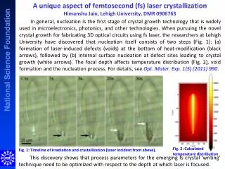
A unique aspect of femtosecond (fs) laser crystallizationHimanshuJain, Lehigh University, DMR 0906763 In general, nucleation is the first stage of crystal growth technology that is widely used in microelectronics, photonics, and other technologies. When pursuing the novel crystal growth for fabricating 3D optical circuits using fs laser, the researchers at Lehigh University have discovered that nucleation itself consists of two steps (Fig. 1): (a) formation of laser-induced defects (voids) at the bottom of heat-modification (black arrows), followed by (b) internal surface nucleation at defect sites leading to crystal growth (white arrows). The focaldepth affects temperature distribution (Fig. 2), void formation and the nucleation process. For details, see Opt. Mater. Exp. 1(5) (2011) 990. Fig. 2: Calculated temperature distribution Fig. 1: Timeline of irradiation and crystallization (laser incident from above). • This discovery shows that process parameters for the emerging fs crystal ‘writing’ technique need to be optimized with respect to the depth at which laser is focused.
A new laser crystallization facility is nucleatedHimanshuJain, Lehigh University, DMR 0906763 To promote the concept of ‘laser writing’ for broad range of applications in glasses and crystals, a dedicated continuous-wave laser crystallization system has been nucleated at Lehigh University. It is available to students and researchers from diverse backgrounds in Materials Science & Engineering, Physics and Electrical Engineering departments. Currently, the system includes a 488 nm laser with tunable power, 50x objective lens, digital camera, and XYZ stage (Fig. 1(a)), with custom interface capable of producing bends and smooth curves (Fig. 1(b)). It is being expanded to accommodate new functions like in-situ Raman spectroscopy. Interested researchers can modify the surface region of solids for specific functionality. (c) (a) (b) Fig. 1: (a) Laser optics and stage setup, (b) the laser control allows fabrication of complex shapes, and (c) example of crystalline lines of widely used LiNbO3as written in a glass.