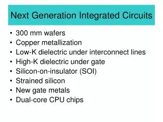
Next Generation Integrated Circuits
Discover the forefront of semiconductor technology with next-generation integrated circuits (ICs) featuring 300 mm wafers, advanced copper metallization, and innovative dielectric materials. We explore low-K dielectrics under interconnect lines and high-K dielectrics under gates, alongside silicon-on-insulator (SOI) and strained silicon techniques that enhance performance. Emphasizing new gate metals and dual-core CPU architecture, our insights highlight key benefits like reduced leakage currents and improved carrier mobility for superior device efficiency.

Next Generation Integrated Circuits
E N D
Presentation Transcript
Next Generation Integrated Circuits • 300 mm wafers • Copper metallization • Low-K dielectric under interconnect lines • High-K dielectric under gate • Silicon-on-insulator (SOI) • Strained silicon • New gate metals • Dual-core CPU chips
Next Generation Integrated Circuits • 300 mm wafers • Copper metallization • Low-K dielectric under interconnect lines • High-K dielectric under gate • Silicon-on-insulator (SOI) • Strained silicon • New gate metals • Dual-core CPU chips
Next Generation Integrated Circuits • 300 mm wafers • Copper metallization • Low-K dielectric under interconnect lines • High-K dielectric under gate • Silicon-on-insulator (SOI) • Strained silicon • New gate metals • Dual-core CPU chips
High-K Gate Dielectric • Reduced fringing of gate electric field – better switching control, less leakage current • Reduced tunneling leakage current with thin oxides • Si3N4, ZrO2, HfO2
Next Generation Integrated Circuits • 300 mm wafers • Copper metallization • Low-K dielectric under interconnect lines • High-K dielectric under gate • Silicon-on-insulator (SOI) • Strained silicon • New gate metals • Dual-core CPU chips
Silicon-On-Insulator • No p-n junction for electrical isolation • Reduced inter-device coupling • Reduced parasitic capacitance • No deep diffusion required for isolation - less fabrication time,closer device packing
Next Generation Integrated Circuits • 300 mm wafers • Copper metallization • Low-K dielectric under interconnect lines • High-K dielectric under gate • Silicon-on-insulator (SOI) • Strained silicon • New gate metals • Dual-core CPU chips
Strained Silicon • Enhanced carrier mobility – compensates for increased ionized impurity scattering in thin, heavily-doped layers
Next Generation Integrated Circuits • 300 mm wafers • Copper metallization • Low-K dielectric under interconnect lines • High-K dielectric under gate • Silicon-on-insulator (SOI) • Strained silicon • New gate metals • Dual-core CPU chips
New Generation ICs at Intel Main Page http://www.intel.com/technology/silicon/index.htm Reports and Publications http://www.intel.com/technology/silicon/research.htm?iid=tech_sil+rd
New Generation ICs at AMD Processor Cores Roadmap http://www.thinkcp.com/AMD/roadmap.html Main Page http://www.amd.com/us-en/
New Generation ICs at AMD Back to Main
New Generation ICs at IBM Main Page http://www.research.ibm.com/ Nanofabrication http://www.ibm.com/search/?en=utf&v=11&lang=en&cc=&lv=w&q=%2BNanofabrication%20%2Burl.all:research.ibm.com Reports and Publications http://www-916.ibm.com/press/prnews.nsf/jan/0C17FDCBF4B76CE185256C6F0064206D