Download
1 / 46
470 likes | 676 Views
Silicon Detectors - I. B.G. Svensson University of Oslo, Department of Physics, Physical Electronics, P.O. 1048 Blindern, N-0316 Oslo, NORWAY and University of Oslo, Centre for Materials Science and Nanotechnology P.O. 1128 Blindern, N-0318 Oslo, NORWAY. Department of Physics.

E N D
Silicon Detectors - I B.G. Svensson University of Oslo, Department of Physics, Physical Electronics, P.O. 1048 Blindern, N-0316 Oslo,NORWAY and University of Oslo, Centre for Materials Science and Nanotechnology P.O. 1128 Blindern, N-0318 Oslo, NORWAY Department of Physics IRTG, Heidelberg Oct-06
Micro- and Nanotechnology Laboratory (MiNaLab), 5000 m2, OSLO (April-2004)
MiNa-lab ...inside
Staff at MiNa PhD students Post-doctors/Researchers ’Permanent’ Giovanni Alfieri Jens S. Christensen Viktor Bobal, engineer Marc Avice Ulrike GrossnerTerje G. Finstad, prof Jan H. Bleka Philip Y.Y. Kan Liv Furuberg, ass. prof (adj) Thomas Moe BørsethEduoard V.MonakhovA. B. Hanneborg, ass. prof (adj) Ingelin ClausenLeonid MurinAndrej Yu. Kuznetsov, ass. prof K-M. JohansenIoana PintilieThomas Martinsen, engineer Matthieu Lacolle Alexander Ulyashin Ola H. Sveen, ass. prof Jeyanthinath Mayandi 2 New Post-docsBengt G. Svensson, prof Mads MikelsenAasmund Sudbø, prof (UNIK) Ramon Schifano David I. Wormald, eng. (30 %) Lasse Vines 2 New PhD students ~6 MSc students, Visitors Jan-2006
Outline • Some fundamentals about materials, device physics and processing related to Si detectors • Radiation tolerance of Si detectors, limiting factors • Defect/impurity engineering of Si detectors • New detector structures ITRG, Heidelberg Oct-06
7 mm Al SiO2 n– p+ 300 µm n+ ‘Baby detector’ p+-n–-n+ Si detectors MeV/GeV particles, radiation n-~ (2-5)x1012 cm-3 Cf ni ~ 1.5x1010 cm-3 @ RT p+, n+ by ion implantation ICT/Department of Microsystems and Nanotechnology
Department of Physics/Physical Electronics MeV ion accelerator at UiO/MiNa-lab Ion implantation and RBS-analysis National Electrostatics Corporation, 1 MV terminal voltage
Basic considerations (zero bias) p+ n- n+ W = (2eV0(Na+Nd)/q(Na+Nd))½ - depletion region Na>>Nd W = (2eV0/(qNd))½ ≈ 20 mm LD = (ekT/q2Nd)½ ≈ 3 mm- Debye length at RT
Basic considerations (full (over) depletion) p+ n- n+ W ≈ 300 mm Vreversebias ≈ 135 V Vbias Ldrift = mE t If: Ldrift~150 mm Eaverage~5x10³ V/cm thole≈6 ns E0 ≈ 1x10⁴ V/cm (E0(max)=2x10⁵ V/cm) ℰ-field
Silicon particle detectors 0 V, pre-amp. • Advantages: • high signal-to-noise ratio • fast direct charge readout • high spatial resolution p+ e h n- e h e h n+ Ubias - p+ - - + + n+ +
Signal formation p+ hole 280 mm electron n+ Contribution of drifting carriers to the total induced charge depends on DUw ! Simple in diodes and complicated in segmented devices! For track: Qe/(Qe+Qh)=19% in ATLAS strip detector diode Qh=Qe=0.5 q ATLAS SD G. Kramberger, Trapping in silicon detectors, Aug.23-24, 2006, Hamburg, Germany
Outline • Some fundamentals about materials, device physics and processing related to Si detectors • Radiation tolerance of Si detectors, challenges and limiting factors • Defect/impurity engineering of Si detectors • New detector structures ITRG, Heidelberg Oct-06
Reliable detection of mips S/N ≈ 10 reachable with Experimental requestDetector property Proton-proton collider Energy: 2 x 7 TeV Luminosity: 1034 Bunch crossing: every 25 nsec Rate: 40 MHz pp-collision event rate: 109/sec (23 interactions per bunch crossing) Annual operational period: 107 sec Expected total op. period: 10 years LHC properties period of 10 years low dissipation power atmoderate cooling Silicon pixel and microstrip detectors meet all requirements for LHC How about future developments? LHC-Challenge for Tracking Detectors employing minimum minimum detectorthickness material budget High event rate excellent time- (~10 ns) & high track accuracy & position resolution (~10 µm) Silicon Detectors: Favorite Choice for Particle Tracking Example: Large Hadron Collider LHC, start 2007 • Proton-proton collider, 2 x 7 TeV • Luminosity: 1034 • Bunch crossing: every 25 nsec, Rate: 40 MHz • event rate: 109/sec (23 interactions per bunch crossing) • Annual operational period: 107 sec • Expected total op. period: 10 years LHC properties Experimental requests Detector properties Reliable detection of mips S/N ≈ 10 High event rate time + positionresolution: high track accuracy~10 ns and ~10 µm Complex detector design low voltage operation in normal ambients Intense radiation field Radiation tolerance up to during 10 years 1015 hadrons/cm² Feasibility, e.g.large scale availability 200 m² for CMSknown technology, low cost ! Silicon Detectors meet all Requirements ! G. Lindström et al. Intense radiation field Radiation tolerance up to throughout operational 1015 1MeV eq. n/cm²
5 years 10 years 2500 fb-1 500 fb-1 Main motivations for R&D on Radiation Tolerant Detectors: Super - LHC • LHC upgradeLHC (2007), L = 1034cm-2s-1f(r=4cm) ~3·1015cm-2 • Super-LHC (2015 ?), L = 1035cm-2s-1f(r=4cm) ~1.6·1016cm-2 • LHC (Replacement of components)e.g. - LHCb Velo detectors (~2010) - ATLAS Pixel B-layer (~2012) • Linear collider experiments (generic R&D)Deep understanding of radiation damage will be fruitful for linear collider experiments where high doses of e, g will play a significant role. 5 CERN-RD48 CERN-RD50 G. Lindström et al.
Radiation Damage in Silicon Detectors Two types of radiation damage in detector structures: Bulk (Crystal) damagedue to Non Ionizing Energy Loss (NIEL - displacement damage, built up of crystal defects – I. Increase of leakage current (increase of shot noise, thermal runaway) II. Change of effective doping concentration(higher depletion voltage, under- depletion) III. Increase of charge carrier trapping(loss of charge) • Surface damagedue to Ionizing Energy Loss (IEL)- accumulation of charge in the oxide (SiO2) and Si/SiO2 interface – affects: interstrip capacitance (noise factor), breakdown behavior, … ! Signal/noise ratio = most important quantity ! G. Lindström et al.
Trapping and recombination of carriers Schockley and Read, Phys. Rev. 87, 835 (1952)
Deterioration of Detector Properties by displacement damage NIEL Dominated by clusters Point defects + clusters Damage effects generally ~ NIEL, however differences betweenproton&neutron damage important for defect generation in silicon bulk
Radiation Damage – Leakage current with time (annealing): 80 min 60C Increase of Leakage Current …. with particle fluence: • Leakage current decreasing in time (depending on temperature) • Strong temperature dependence: • Damage parameter (slope in figure)Leakage current per unit volume and particle fluence • is constant over several orders of fluenceand independent of impurity concentration in Si can be used forfluence measurement Consequence:Cool detectors during operation! Example: I(-10°C) ~1/16 I(20°C) G. Lindström et al.
…. with time (annealing): Short term: “Beneficial annealing”Long term: “Reverse annealing” - time constant depends on temperature:~ 500 years (-10°C)~ 500 days ( 20°C)~ 21 hours ( 60°C) Radiation Damage – Effective doping concentration Change of Depletion Voltage Vdep (Neff) …. with particle fluence: „Hamburg model“ “Type inversion”: Neff changes from positive to negative (Space Charge Sign Inversion) before inversion afterinversion p+ n+ n+ p+ Consequence:CoolDetectors even during beam off (250 d/y)alternative: acceptor/donor compensation by defect enginrg. G. Lindström et al.
Charge trapping & recombination - p+ - - + + + n+ • Increase of charge collection time • Decrease of the charge collection efficiency • Decrease of the S/N ratio
….. and change with time (annealing): Radiation Damage – Charge carrier trapping Deterioration of Charge Collection Efficiency (CCE) by trapping Trapping is characterized by an effective trapping time eff for electrons and holes: where: Increase of inverse trapping time (1/) with fluence Charge trapping leads to very small le,h at Feq = 1016/cm² Consequence:Cooling does not help but:use thin detectors (~100mm) and p-type Si G. Lindström et al.
„Executive Summary“ • Si-Detectors in the inner tracking area of future colliding beam experiments have to tolerate hadronic fluences up to Feq = 1016/cm² • Deterioration of the detector performance is largely due to bulk damage caused by non ionizing energy loss (NIEL) of the particles • Reverse current increase (most likely due to both point defects and clusters) is effectively reduced by cooling. Defect engineering so far not successful • Change of depletion voltage is severe, also affected by type inversion and annealing effects. Modification by defect engineering is possible, for standard devices continuous cooling is essential (‚freezing‘ of annealing) • Charge trapping is possibly the ultimate limitation for Si-detectors, responsible defects are unknown, cooling and annealing have minor effects
Outline • Some fundamentals about materials, device physics and processing related to Si detectors • Radiation tolerance of Si detectors, challenges and limiting factors • Defect/impurity engineering of Si detectors • New detector structures ITRG, Heidelberg Oct-06
The RD50 Collaboration RD50: Development of Radiation Hard Semiconductor Devices for High Luminosity Colliders 1. Formed in November 2001 2. Approved by CERN in June 2002 (http://rd50.web.cern.ch/rd50/) • Main objective: • Development of ultra-radiation hard semiconductor detectors for the luminosity upgrade of LHC to 1035 cm-2s-1 (S-LHC) • Challenges: • - Radiation hardness up to fluences of 1016 cm-2 required; • - Fast signal collection (10 ns); • - Cost effectiveness. Presently 280 Members from 55 Institutes Belgium (Louvain), Canada (Montreal), Czech Republic (Prague (2x)), Finland (Helsinki (2x), Oulu), Germany (Berlin, Dortmund, Erfurt, Halle, Hamburg, Karlsruhe), Greece (Athens), Israel (Tel Aviv), Italy (Bari, Bologna, Florence, Milano, Modena, Padova, Perugia, Pisa, Trento, Trieste, Turin), Lithuania (Vilnius), Norway (Oslo (2x)), Poland (Warsaw), Romania (Bucharest (2x)), Russia (Moscow (2x), St.Petersburg), Slovenia (Ljubljana), Spain (Barcelona, Valencia), Sweden (Lund) Switzerland (CERN, PSI), Ukraine (Kiev), United Kingdom (Exeter, Glasgow, Lancaster, Liverpool, London, Sheffield, University of Surrey), USA (Fermilab, Purdue University, Rutgers University, Syracuse University, BNL, University of New Mexico)
Radiation effects in silicon detectors Damage of the crystal lattice Si atom (Sis) Electronic levels of main electron traps in Si: V VO V2 Ec -/0 =/- Ec-0.23 eV Ec-0.18 eV Cs I -/0 Ec-0.44 eV 0/+ Ev+0.20 eV Oi Ev
Main types of Si-detector materials used • Float zone (Fz); low oxygen and carbon content, [Oi]<5x1015 cm-3 and [Cs]<5x1015 cm-3 • Diffusion oxygenated Fz (DOFZ), [Oi]~3x1017 cm-3 and [Cs]<5x1015 cm-3 • Magnetic Czochralski (MCz), [Oi]~7x1017 cm-3 and [Cs]<5x1015 cm-3 • Epitaxial layers (Epi) on highly doped substrates, [Oi]<5x1015 cm-3 and [Cs]<5x1015 cm-3
Impurity engineering of high-purity Si Silicon Oxygen (Oi) Interstitial configuration Vacancy oxygen (VO) center (0/-) EC 0.18 eV EV
Interstitial carbon (Ci) Three different charge states (-,0,+) EC - 0.10 eV 0 + 0.27 eV EV Cs has a strong impact on the overall defect generation via its role as I-trap; Cs + I Ci Carbon is of key importance in n-/p- detector layers, either directly or indirectly G. Davies and R.C. Newman, Handbook of Semiconductors, Eds T.S. Moss, S. Mahajan (Elsevier, Amsterdam, 1994) ch. 21, p. 1557
Evolution of Ci at RT; an illustration Fz (~15 Ωcm) [Oi]~1.2x1016 cm-3 [Cs]≤5x1015 cm-3 Lalita et al., NIMB 120, 27 (1996)
(Ci) Cf value by Tipping, Newman, Semicond. Sci. Techn. 2, 315 (1987) DCi = 0.4exp(-0.87(eV)/kT) cm2/s Lalita et al., NIMB 120, 27 (1996)
Purpose of defect engineering VO V2 Ec -/0 =/- Ec-0.18 eV Ec-0.23 eV -/0 Ec-0.44 eV 0/+ Ev+0.20 eV Ev V + Oi VO V + V V2 Leakage current as a function of the bias in silicon detector with different types of defects (SILVACO TCAD). Monakhov et al., Sol. St. Phen. 82-84, 441 (2002) Suppress formation of defects with levels close to mid-gap !!
Key defect reactions and why oxygenation V + I Ø (only a few % survive) I + CsCi Ci + Cs CsCi Ci + Oi CiOi …… V + Oi VO V + VO V2O V + V V2 V + Vn Vn+1 (n2) Cs traps (’immobolizes’) I and suppresses self-annihilation ☹ Oi traps V and suppresses V-clustering ☺ (Standard interpretation of oxygenation effect….)
Impurity engineering of high-purity Si High [Cs] DOFZ
g-irradiated Si-detectors I-center Ec-0.545 eV sn = 1.7x10⁻¹⁵ cm2 sh =9x10-14 cm2 Key defect for space charge inversion,… Identity of I?? I. Pintilie at al., Appl. Phys. Lett. 81, 165 (2002)
g-irradiated Si-detectors The I-center has a quadratic dose dependence ’simple’ cluster-type defect I. Pintilie at al., Appl. Phys. Lett. 82, 2169 (2003)
No radiation hardening for neutrons Oxygenation does not affect direct cluster formation!?
Improving Si radiation hardness Magnetic Czochralski (MCZ) silicon standar FZ-Si: [O]~1016 cm-3 oxygenated FZ-Si: [O]~1-4x1017 cm-3 MCZ-Si: [O]~1018 cm-3 Higher radiation tolerance... ...but the same 'neutron problem'.
Summary of defect/impurity engineering • Oxygenation (shallow VO instead of deep levels) • Decrease in carbon content (C effects vacancy- interstitial annihilation) argument for epi-detectors • Hydrogenation (H passivates dangling Si bonds) • Formation of electrically inactive extended defects (sink for vacancies and interstitials) • Engineering of ’direcly created’ clusters (neutron irradiation) is a challenge…
Outline • Some fundamentals about materials, device physics and processing related to Si detectors • Radiation tolerance of Si detectors, challenges and limiting factors • Defect/impurity engineering of Si detectors • New detector structures ITRG, Heidelberg Oct-06
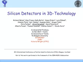
3D detectors • Proposed by S.I. Parker, C.J. Kenney and J. Segal (NIM A 395 (1997) 328) • Called 3-D because, in contrast to silicon planar technology, have three dimensional (3-D) electrodes penetrating the silicon substrate • Presently, a joint effort exists between Brunel Univ., Hawaii Univ., Stanford Univ., SINTEF and UiO Conventional (a) and 3D (b) detectors: a) b) depletion thickness depends on p+ and n+ electrode distance, not on the substrate thickness (1) can operate at very low voltages or (2) can have a high doping for ultra-high radiation hardness, and (3) short distance for charge collection
3D detectors Charge collection in 3D detectors • shorter collection length than planar technology • shorter charge collection time than planar technology • higher charge collection efficiency computer simulations of the charge collection dynamics for planar and 3D detectors
3D detectors Real devices a 3D detector structure: a 3D structure etched at SINTEF: 15 m 200 m 4 m
Semi-3D detectors Proposed by Z. Li(NIM A 478 (2002) 303). Single-side detectors with alternating p- and n- strips on the front side After SCSI, the depletion occurs from both sides reducing the needed depletion voltage by factor 2.5
FINAL SUMMARY • There is considerable activity and progress in improving radiation hardness of Si particle detectors, reaching 1016 cm-2(1 MeV n eq.) is, indeed, a challenge • Using the so-called defect/impurity engineering, the range of working fluences has been extended up to >1015 cm-2 • The progress in semiconductor microtechnology allows design of detector structures with 'inherent' ultra-high radiation tolerance; development of a viable industrial ‘3D technology’ is in progress