Download
1 / 29
290 likes | 334 Views
This paper discusses advancements in 3D silicon detectors for high-energy physics experiments, focusing on radiation hardness and performance in future particle collider upgrades. 3D designs aim to overcome challenges posed by increased radiation doses, offering superior collection efficiency and reduced trapping effects. Various 3D detector types, simulations, and practical applications are explored, highlighting their potential for inner tracking systems in the Super-LHC era. The study showcases the evolution of 3D detector technology and its implications for enhancing data acquisition in particle physics.

E N D
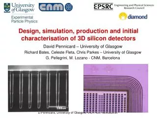
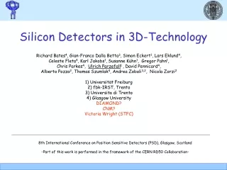
Silicon Detectors in 3D-Technology Richard Bates4, Gian-Franco Dalla Betta3, Simon Eckert1, Lars Eklund4, Celeste Fleta4, Karl Jakobs1, Susanne Kühn1, Gregor Pahn1, Chris Parkes4, Ulrich Parzefall1 , David Pennicard4, Alberto Pozza2, Thomas Szumlak4, Andrea Zoboli3,2, Nicola Zorzi2 1) Universität Freiburg 2) fbk-IRST, Trento 3) Universita di Trento 4) Glasgow University DIAMOND? CNM? Victoria Wright (STFC) 8th International Conference on Position Sensitive Detectors (PSD), Glasgow, Scotland -Part of this work is performed in the framework of the CERN RD50 Collaboration-
to do • new eff plots from Gregor Ulrich Parzefall, Universität Freiburg
Introduction • Motivation LHC luminosity upgrade: SLHC • 3D Detectors 1997 • Ten years later: 3D Projects in RD50 & ATLAS • Conclusions & Outlook 3D Detector Idea: Parker, Kenny, Segal, NIM A395, (1997) 328 Disclaimer: At VERTEX 2008, Chris Parkes presented an overview of 3D detectors, see: http://indico.cern.ch/conferenceDisplay.py?confId=30356 Chris extensively covered 3D pixel detectors and processing. I will concentrate on XXX . Other 3D talks: J. Marchal “Synchrotron x-ray applications of pixel/strip detectors at Diamond” G. Pellegrini “Fabrication and simulation of Novel Ultra Thin 3D Silicon Detector - Plasma Diagnostics” Ulrich Parzefall, Universität Freiburg
Motivation: The SLHC from Ian Dawson • LHC Upgrade to Super-LHC (SLHC) planned in 2015: • Increase luminosity by factor ten compared to LHC • Massive increase of radiation dose for silicon detectors, making radiation damage the major concern • ATLAS will need to replace Inner Tracking system to cope with SLHC • Not clear if radiation hardness of planar Silicon pixel or strip detectors is sufficient • extremely challenging radiation environment for inner tracking detectors • 3D designs investigated for SLHC pixel detectors • Study 3D short strip detectors (~2-3cm strip length) Ulrich Parzefall, Universität Freiburg
Reminder: The 3D Principle n-columns p-columns wafer surface PLANAR 3D p+ p+ p+ n+ 50 mm - 300 mm n-type substrate - - - - - - - - - + + + + + + + + + + • 3D detectors decouple thickness (=signal) and depletion voltage • Depletion and charge collection is sideways • Superior radiation hardness “by design” • less trapping (as collection distances are short) • Full depletion voltage less affected by growing acceptor concentration (Vdep ~ distance2) • Original 3D designs • Brilliant but complex • conceived as pixel devices • can connect rows of columns to form strips Ulrich Parzefall, Universität Freiburg
3D Results Overview • Summary of results from planar and 3D detectors by Cinzia • superior radiation hardness (ATLAS 3D pixel collaboration) • Results for 3D strip detectors above 1015Neq still unavailable Ulrich Parzefall, Universität Freiburg
3D Designs 230 columns → 18.4 mm bias ring guard ring n+ columns • Original 3D • Good performance but costly and complex to manufacture • Mainly made for pixel applications • Single Type Column (STC) 3D • Much simpler: columns on one side only • Produced successfully: Pixel and strip detectors exist • STCs tested extensively • Double Type Column (DTC) 3D • Better than STC, yet simpler than classic 3D • The next step in “simpler 3Ds” 3D STC strip detector Ulrich Parzefall, Universität Freiburg
3D Single Type Columns Design metallisation oxide n+ 300 µm P+ -stop p p+ metallisation MIP e h 150µm Holes drift in the central region and diffuse towards backside contact n+ elektrode n+ electrode Electrons are swept away by the transversal field 150µm Cross section between two electrodes: • Single Type Column (STC) 3D design: • Columns not completely etched through wafer no support wafer necessary • STC sensors made by FBK-irst (Trento) • Processing less complex and costly compared to standard 3D • Si bulk can be n-in-p material • no type-inversion • Collection of e- (faster, less trapping) • Wafers: Czochralski or Floatzone-Si • P-spray or p-stop isolation (to avoid conductive layer between n-implants) • Low field region exists (slow drift) • field given by doping level (not Ubias) • LHC is fast, so expect reduced CCE at 40 MHz • 3D STC strip designs interesting for innermost strip layers • 3D STC strip detectors are “like planar strips plus columns under the strips” Piemonte et al. NIMA 541 (2003) 441 Ulrich Parzefall, Universität Freiburg
3D stc Simulations – Depletion 1) Ubias=0V 2) Ubias=2V xy-null field lines 4) Ubias=20V 3) Ubias=5V • Initial fast lateral depletion at 5V for FZ Si • Then depleting like a planar detector • Low field in central region remains • indep. of bias voltage • bias affects only field under columns towards back side Ulrich Parzefall, Universität Freiburg
3D STC Module with FZ sensors carbon for cooling ATLAS SCT electronics Rebondable Fan-ins 3D-sensor Sensor part Electronics part • 3D sensors • 80μm strip pitch, 80μm column pitch • 300μm thick • 64 strips, 2cm strip length • Si: FZ p-spray or FZ p-stop FZ p-stop sensor ~ 20 mm Ulrich Parzefall, Universität Freiburg
Noise Behaviour Lateral depletion noise in ke- planar detector-like depletion Unbonded channels' noise noise in ke- Unbonded 3D stc sensor • 3D devices will have higher capacitance (and noise!) than planar designs • Capacitance shows frequency dependence • Measure noise at LHC readout speed (40MHz) • Noise is • Uniform across sensor • Rapidly decreasing with bias voltage until lateral full depletion at ≈ 25V • Then slowly decreasing as sensor continues to deplete towards backside • Typical noise 1200 ENC(corresponds to 6-7cm strips in planar design) • Micro-discharge starting at 95V (before sensor is fully depleted) Unbonded noise in ke- Full lateral depletion Ulrich Parzefall, Universität Freiburg
Three methods available to generate charge in Si: Laser Radioactive source High-energy particles (MIP) Example: pulsed IR Laser Focused to 5μm spot size Coupled into fiber Scan detector surface to study uniformity of charge collection efficiency Scan area is unit cell Narrow region of lower CCE (≈5µm) on p-spray sensor Likely cause is central low field region Signal drops by ≈25% - 30% Signal: IR Laser Measurements 80 µm y x 80 µm Laser scan area Ubias= 80V Ulrich Parzefall, Universität Freiburg
Signal: Source • 3D-STC modules tested with e- from Sr90 beta source • Test before and after irradiation to 1015Neq/cm2 • Charge collection is reduced by irradiation, and also slightly by annealing • Given sufficient HV stability, the irradiated detector collects the same charge as prior to irradiation • VFD ~ 230V as predicted for CZ p-type 3D STC on CZ p-type Si Expected VLAT = 33V Expected VFD = 230V Ulrich Parzefall, Universität Freiburg
2007 Beam Test • Two 3D STC detectors were tested with 180GeV SPS Pions in Autumn 2007 • Main aim: position-resolved study of CCE, signal and signal shape • Signal measurement with ADC Calibration:Landau MPV at 2.4 fC(70% of 3.5 fC) • Note: Entire Test Beam analysis still preliminary (work on tracking & alignment ongoing) Track y [mm] Track x [mm] ADC Value Ulrich Parzefall, Universität Freiburg
Efficiency in Beam Test plot range 80 µm residual Strip centre • Alignment much better orthogonal to strips due to small beam shape • Study 1-D efficiency orthogonal to strip • number of hits on 3D matched to tracks as a function of distance to strip „residual“ • map entire detector onto one strip • Low efficiency at • large distance to strip: low field region • strip center: no charge deposition in hollow columns Note: only relative efficiency is measured! Absolute eff. higher due to DAQ desynchronisation, dead strips Strip centre Ulrich Parzefall, Universität Freiburg
Efficiency in Beam Test • Can also study 1-D efficiency parallel to strip • “Looking for columns“ • Map entire detector onto one 300μm long cell • Restrict to hits 10μm each side of strip centre • Structure with 100μm spacing is visible, but washed out due to • Track Resolution • Tilt angle and angle uncertainty Ulrich Parzefall, Universität Freiburg
Efficiency 80 µm residual x 300 µm • Repeat study also in 2D • Fold all data onto one small cell (80μm x 300 μm) • Inter-strip regions coincide with steep drop to lower efficiency • Columns just about visible as low efficiency areas? • Testbeam analysis still ongoing with improved tracking, re-alignment and more statistics Ulrich Parzefall, Universität Freiburg
Opposite Polarity Signals 80 µm y x 80 µm IR-Laser • Opposite polarity signals get induced on neighbouring strips • Seen very clearly in Laser • Also visible in Beam Test • Traditional clustering algorithms would fail • Effect only observable for neighbouring strips, but must also be present within one strip -> low charge signals • Reason is field configuration • charges drift mainly sideways to/away from columns • low field means slow hole drift to backside, tdrift >25ns Vbias = 10V Beam Test: Signal on neighbour Ulrich Parzefall, Universität Freiburg
Comments on 3D-STCs • Overall charge level low (2.2fC) due to ballistic deficit arising from 3D-STC field configuration • 3D-STC after irradiation to 1015Neq/cm2 are still operational • Same CCE as unirradiated device, but at much higher bias voltage • The annealing has affected the CCE: • On CZ probably due to trapping of holes between columns • On FZ mostly because the annealing was too long and Neff has increased significantly • Modules recently taken to another irradiation step, total dose now ~2.5·1015Neq/cm2 Signal shapes from 2007 test beam Signal [ADC counts] Need to move from STC to DTC! Ulrich Parzefall, Universität Freiburg
Double-sided 3D detectors p+ 300um n+ p+ 300um n+ DTC STC • 3D STC designs were first steps towards simple cost-effective 3Ds • Main problem: low field regions, and independence of field from bias voltage • Improved 3D structure proposed by G. Pellegrini (CNM): n- and p-type columns etched from opposite sides • Similar design produced independently by FBK-irst (Trento) • Columns do not pass through full substrate thickness • Reduces low field regions, field becomes driven by bias voltage • Expect faster signals and higher CCE • Simulations indicate DTC is a rather radiation hard design, and compares well to conventional 3D design • 3D DTC structures from both manufacturers in 2008 beam test (CMS with Panja Luukka, Helsinki et al) Ulrich Parzefall, Universität Freiburg
Double Type Column Detectors: DDTC • First detectors • Simulations… Ulrich Parzefall, Universität Freiburg
First DTC Results: Strip detector IV Post-Irradiation to 1015Neq Pre-Irradiation • 128 strips, 50 holes/strip, pitch 80μm, length 4mm • Measured with 3 strips and guard ring at 0V, and backside biased • Strip currents ~100pA (T=21˚C) in all 4 detectors • Can reliably bias detectors to 50V (20 times lateral depletion voltage), no breakdown • Capacitance 5pF / strip • Guard ring currents vary: • Highest 20μA at 10V • Lowest 0.03μA at 50V • Irradiated with 5·1015 Neq in Ljubljana • IV curves roughly as expected for fluence Ulrich Parzefall, Universität Freiburg
Conclusions & Outlook • Extensive tests on modules with STC 3D detectors (STC originally intended as technology test) • STCs are functional detectors, and radiation hard • Too slow for a 40 MHz SLHC (field configuration) • Still have some STC measurements in the pipeline • Two modules irradiated to 2.5·1015Neq/cm2 in source and laser test systems • Completion of 2007 test beam analysis • Radiation hardness of planar designs can be increased with equivalent 3D design • higher noise, higher price • ATLAS has large 3D program for pixel detector underway • Future 3D tests will concentrate on DTC devices • Simulations and first tests indicate faster charge collection Related Talks: XXX Ulrich Parzefall, Universität Freiburg
BACKUP ONLY Ulrich Parzefall, Universität Freiburg
2µm step size 50µm×50µm area y-axis along the strips At variable bias voltage High Resolution Laser Scan y 80 µm Vbias = 25V 80 µm x Vbias = 50V Vbias = 75V • Width independent of bias for Vbias > 25V