Download
1 / 20
200 likes | 403 Views
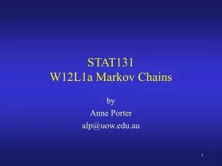
Readout schemes. Translator. DAQ VME CRAMS Sequencer. DET. FEE. FEE. Gasiplex. Analog Buffer. FEE. FEE. FEE. FEE. MANAS. MANAS. MANAS. MANAS. Readout –STAR PMD No of channels = 82944 One chain reads 1728 chs. No of Chains =48

E N D
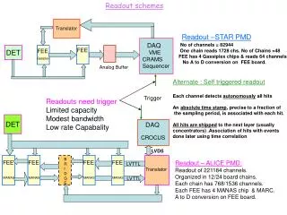
Readout schemes Translator DAQ VME CRAMS Sequencer DET FEE FEE Gasiplex Analog Buffer FEE FEE FEE FEE MANAS MANAS MANAS MANAS Readout –STAR PMD No of channels = 82944 One chain reads 1728 chs. No of Chains =48 FEE has 4 Gassiplex chips & reads 64 channels. No A to D conversion on FEE board. Alternate : Self triggered readout Each channel detects autonomously all hits An absolute time stamp, precise to a fraction of the sampling period, is associated with each hit. All hits are shipped to the next layer (usually concentrators) .Association of hits with events done later using time correlation Trigger Readouts need trigger Limited capacity Modest bandwidth Low rate Capabality DET DAQ CROCUS LVDS B R I D G E Readout – ALICE PMD: Readout of 221184 channels. Organized in 12/24 board chains. Each chain has 768/1536 channels. Each FEE has 4 MANAS chip & MARC. A to D conversion on FEE board. LVTTL Translator LVTTL
Buffer L1 Select L2 Select DAQ – Data Push Architecture Detector Self-triggered front-end Autonomous hit detection time distribution FEE No dedicated trigger connectivity All detectors can contribute to L1 Cave Shack Highbandwidth DAQ Large buffer depth available System is throughput-limitedand not latency-limited Some Programmable Logicand mostly CPU's Use term: Event Selection Archive
READ-OUT ASIC s for CBM Expt.. • ASIC s developed for DETNI (DET for Neutron Instrumentation) • MSGCROC –Self Triggered ASIC for readout of MSGC detector -32 Channel • N-XYTER- Neutron, X, Y, Time and Energy Readout Chip- 128 channel (self triggered) . • Front-end • 128(32) channels, charge sensitive pre-amplifier, both polarities • 30 pF detector capacitance, ENC 1000 e • self-triggered, autonomous hit detection • time stamping with 1 ns resolution (needed to correlate x-y views) • Readout • energy (peak height) and time information for each hit • data driven, de-randomizing, sparsifying readout • 32 MHz average hit rate • 128 channel version (Si,GEM): ~ 250 kHz hit / channel • 32 channel version (MSGC): ~ 1 MHz hit / channel
Readout Data rates:
MSGCROC –Block diagram 1) Thresh voltage for comparator generated internally by 8 bit DAC 2) 5 bit DAC to compensate threshold offset on each channel and corrects threshold voltage. 3) 14 bit time stamp signature by combination of 12 bit gray code counter,toggle FF & buffered I/P CLK 4) Chips slow control interface using I2C bus. • Readout channel after pre- amp split into amplitude (E) in PD & Timing channels . • Timing channel O/P used to latch a 14 bit time stamp with 2 n sec resolution & enables PD Ckt. • O/P Signals from PD and time stamp are stored in 4 stage FIFO s ( Analog and digital). • Readout of memories using token ring based MUX . • This ensures only non zero data are read from buffers (data sparsification)
14 bit gray counter
Input clock signals & Time stamp generation Readout Clocks 1)32 MHZ used in TOKEN,,Memories, ANALOG MUX available on LVDS pins. 2)128 MHZ used for sending digital data out of the chip available on LVDS Pins. 3) Data sent in 4 – 8 bit packets transmitted at 4 times main clk freq i.e 4 *32= 128 MHZ freq
I2C Registers I2C features: 2 bus lines serial data and CLK required Each device addressable by unique address 128 channels by 7 bit address mode 1024 addresses by 10 bit add mode. Serial 8 bit , bidirectional data transfer. Data transfer rate 100 kbps.( standard mode) 46 Registers in total
Testing DC Characteristics 13 mW/channel
Gain & INL with 30 pf Capacitance Fast channel Slow channel Neg Pos Neg Pos 3.86uv/e- Gain 9.49uv/e- 9.2uv/e- 4.26uv/e- INL +/- 4 % +/- 0.5 % +/- 1 % +/- 1 % ENC vs i/p capacitance & Rise time Gain, Noise Specifications Time jitter ENC vs Input Capacitance
Test Results Locations of Test pads Fast shaper Linearity of signal amplitudes - Slow shaper