Synchronization Using Phase-Locked Loops
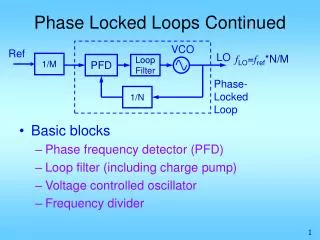
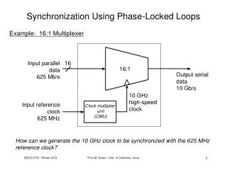
Input parallel data 625 Mb/s. 16. 16:1. Output serial data 10 Gb/s. 10 GHz high-speed clock. Input reference clock 625 MHz. Clock multiplier unit (CMU). Synchronization Using Phase-Locked Loops. Example: 16:1 Multiplexer.

Synchronization Using Phase-Locked Loops
E N D
Presentation Transcript
Input parallel data 625 Mb/s 16 16:1 Output serial data 10 Gb/s 10 GHz high-speed clock Input reference clock 625 MHz Clock multiplier unit (CMU) Synchronization Using Phase-Locked Loops Example: 16:1 Multiplexer How can we generate the 10 GHz clock to be synchronized with the 625 MHz reference clock? Prof. M. Green / Univ. of California, Irvine
Vout + V _ Vin 15R Vf R At DC: Voltage Amplification Ideally, we wish to have Vout = 16·Vin. Let the op-amp be modeled with a 1st-order transfer function: A0 p Prof. M. Green / Univ. of California, Irvine
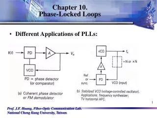
frequency transfer function: Frequency Multiplication feedforward voltage- controlled oscillator Fin frequency detector Fout Vc Ff feedback frequency divider Since frequency ratio is not exactly N, exact synchronization is not possible. Prof. M. Green / Univ. of California, Irvine
A0 0 Achieving Exact Synchronization (1) Consider replacing the amplifier with an ideal integrator: Vout + V _ Vin 15R Vf R Prof. M. Green / Univ. of California, Irvine
Define instantaneous angular frequency: If we can arrange to have the detector respond to phase difference (instead of frequency difference), then integration is naturally introduced into the loop ... Achieving Exact Synchronization (2) Consider a sine function: Prof. M. Green / Univ. of California, Irvine
^ ^ inherent integration exact synchronization Phase-Locked Loop feedforward in voltage- controlled oscillator phase detector Vc f feedback frequency divider ^ Jitter Transfer Function: ^ ^ ^ jitter frequency Prof. M. Green / Univ. of California, Irvine
Jitter frequency fj = Jitter amplitude = = 0.25 UI Illustration of Sinusoidal Jitter Jitter-free clock carrier frequency fc Clock with added jitter Prof. M. Green / Univ. of California, Irvine
input phase step 0 ^ ^ ^ PLL Step Response Example for N = 1: Vin PD Vc VCO Vout ^ ^ Prof. M. Green / Univ. of California, Irvine
^ ^ ^ Loop gain: N Closed-loop transfer function: N Unity-gain frequency: PLL Frequency Response in PD VCO out Vc f Prof. M. Green / Univ. of California, Irvine
vco in PD VCO + ^ out Vc + f lowpass characteristic highpass characteristic Jitter Transfer Functions N 1 0 Prof. M. Green / Univ. of California, Irvine
Disadvantages of 1st-Order PLL • Higher-order transfer function would provide better attenuation of jitter. • Kpd & Kvco have circuit-related constraints; designer would prefer more degrees of freedom. • Phase detector operation requires filtering, which adds poles/zeros to the transfer function. Prof. M. Green / Univ. of California, Irvine
-p +p Detector characteristic is sensitive to both phase and amplitude. Phase Detectors 1. Analog Multiplier Vin, Vf Vd Prof. M. Green / Univ. of California, Irvine
VDD RL RL _ Vout + M1 M1 M1 M1 Vin+ Vin- Vin- Vin+ M2 M2 Vf+ Vf- Large input amplitudes: ISS CMOS Multiplier Realization Small input amplitudes: linear operation Describes an “XNOR” gate... Prof. M. Green / Univ. of California, Irvine
Kpd negative Vin Vd Vf Kpd positive Digital operation allows limiting Vd independent of input amplitudes 2. XNOR (“Digital Multiplier”) - + Vin Vf Vd Prof. M. Green / Univ. of California, Irvine
Properties of XNOR Phase Detector Vin Vd Vf • Useful PD range is [-, 0] • Vd = 0 corresponds to = -/2 steady-state phase offset • In order to extract the average value of Vd, a loop filter is needed... stable equilibrium - + Vswing unstable equilibrium Prof. M. Green / Univ. of California, Irvine
Loop Filters (1) R Vd Vc Consider a simple RC LPF: C −20 dB/decade −40 dB/decade A loop filter is used to average the PD output and provide a higher-order jitter transfer function. 0 reduced, but phase margin also reduced! Resulting jitter peaking is undesirable. 0 dB Prof. M. Green / Univ. of California, Irvine
Loop Filters (2) LPF with added transmission zero: R1 Vd Vc R2 C −20 dB/dec. −40 dB/dec. −20 dB/dec. p z • 0 once again in 1-pole rolloff region no jitter peaking • Parasitic elements will add high-frequency poles; detailed loop simulations required in practice. • Any PLL with one pole at s = 0 is said to be “Type 1.” Prof. M. Green / Univ. of California, Irvine
Steady-State Phase Error ^ Loop gain: Error transfer function: Input frequency step: If then locking cannot occur! |G| Active loop filter: R2 C R1 additional pole at 0 Type II PLL 0 −40 dB/decade −20 dB/decade Prof. M. Green / Univ. of California, Irvine
If the frequencies are close together, periods where Vpd is mostly positive or mostly negative can be observed. Consider the case where fin > ff and both (constant) frequencies are applied to an XOR: Lock Acquisition (1) Vin Vf
Lock Acquisition (2) ^ Suppose initially out < in : Then phase difference moves to the right in the PD characteristic: out increases (correct direction) out decreases (wrong direction) in - out When outincreases, decreases, and slows down. When outdecreases, increases, and speeds up. Prof. M. Green / Univ. of California, Irvine
Lock Acquisition (3) speeds up slows down t speeds up VC VP = “Pull-in voltage” t int loop filter integration time constant initial frequency difference Pull-in time: Since VP > 0, on average out will increase, thereby moving closer to lock After many of these cycles, the frequency is “pulled in.” Prof. M. Green / Univ. of California, Irvine
Lock Acquisition (4) Control voltage transient showing pull-in: fin = 1 GHz Kvco = 5 MHz/V K = 106 rad/sec t = 100 ns fout(0) = 1.002 GHz cycle slips Prof. M. Green / Univ. of California, Irvine
3. Combinational circuit version Idea: Vin Vf Vd PD characteristic: Realization: Vin Vd -p +p Entire region [0,2] now usable! Vf To lengthen the stable region of PD characteristic, we use edge detection instead of level detection: Prof. M. Green / Univ. of California, Irvine
4. Phase-Frequency Detector (PFD) Phase detection behavior: Vin Vin Vup Vf Vup Vdn Vf Vdn Vin leads Vf Vin in phase with Vf Prof. M. Green / Univ. of California, Irvine
PFD Response to Frequency Difference: Vin Vf Vup Vdn -4p -2p +2p +4p PFD exhibits faster frequency acquisition than conventional phase detector. Prof. M. Green / Univ. of California, Irvine
Charge Pump Phase Detector Iout |Zf| Ich -2 2 -Ich z p Vin Vup Ich Iout VC R Vdn Vfb C Cp Ich −20 dB/dec. Prof. M. Green / Univ. of California, Irvine
CMOS Charge Pump Realizations Differential: cmfb Vup Vdn Iout+ Iout- Vup Vdn Vup Vup Vdn Vdn Ich Ich Single-ended: Ich Iout Vup Vdn Ich Prof. M. Green / Univ. of California, Irvine
Type II PLL with PFD & Charge Pump in Ich VCO VC out PFD KVCO fb Ich |G| ^ For : z p −40 dB/dec. −20 dB/dec. −40 dB/dec. Prof. M. Green / Univ. of California, Irvine
Effect of Parasitic Pole p = 10w0 Open-Loop Freq. Response: p = w0/10 p = w0 p = w0 p = 10w0 Closed-Loop Freq. Response: p = w0/10 Larger Cp lower p jitter peaking Prof. M. Green / Univ. of California, Irvine
Measured PLL Locking Design parameters: Settling time (10%) ≈ 15 µs Prof. M. Green / Univ. of California, Irvine
Motivation for CDR: Deserializer (1) Input data Input clock 1:2 DMUX 1:2 DMUX channel 1:2 DMUX If input data were accompanied by a well-synchronized clock, deserialization could be done directly. Prof. M. Green / Univ. of California, Irvine
Motivation for CDR (2) Clock Data retimed data Clock Recovery circuit input data recovered clock PLLs naturally provide synchronization between external and internal timing sources. A CDR is often implemented as a PLL loop with a special type of PD... • Providing two high-speed channels (for data & clock) is expensive. • Alignment between data & clock signals can vary due to different channel characteristics for the different frequency components. Hence retiming would still be necessary. Prof. M. Green / Univ. of California, Irvine
f f RZ spectrum has energy at 1/Tb conventional phase detector can be used. NRZ spectrum has null at 1/Tb ?? Return-to-Zero vs. Non-Return-to-Zero Formats NRZ Tb RZ 0 1 0 1 1 1 0 Prof. M. Green / Univ. of California, Irvine
Vdata Vd VRCK Vdata VRCK Vd Phase Detection of RZ Signals • Phase detection operates same as for clock signals for logic 1. • Vd exhibits 50% duty cycle for logic 0. • Kpd will be data dependent. Prof. M. Green / Univ. of California, Irvine
Vdata Vd VRCK • RZ signals can use same phase detector as clock signals • RZ data path circuitry requires bandwidth that is double that of NRZ. • Different type of phase detection required for NRZ signals. Phase Detection of NRZ Signals Vdata VRCK Vd Since data rate is half the clock rate, multiplying phase detection is ineffective. Prof. M. Green / Univ. of California, Irvine
Idea: Mix NRZ data with delayed version of itself instead of with the clock. Example: 1010 data pattern (differential signaling) Tb X X = = fundamental generated Prof. M. Green / Univ. of California, Irvine
QI QI D CK CK CK CK CK CK CK CK latch: CK Q D CK CK CK Slave Master Operation of D Flip-Flips (DFFs) DFF: CMOS transmission gate: Ideal waveforms: Symbol: D0 D1 D2 D D Q CK Q D0 D1 D2 No bubble Q changes following rising edge of CK Prof. M. Green / Univ. of California, Irvine
DFF Setup & Hold Time At CK rising edge, the master latches and the slave drives. D tsetup thold CK Q When a data transition occurs within the setup & hold region, metastability occurs. Prof. M. Green / Univ. of California, Irvine
QI CK CK CK CK D0 D1 D2 D CK Q D CK CK CK D1 D2 D0 Q CK Slave Master tck-q DFF Clock-to-Q Delay tck-q is determined by delays of transmission gate and inverter. Prof. M. Green / Univ. of California, Irvine
P Din Q RCK synchronized: RCK RCK early: D3 D2 D0 D1 D3 D0 D1 D1 D3 D2 D2 D3 D0 D1 D0 D2 Delay between Din to Q is related to phase between Din & RCK Realization of Data/Data Mixing : Same as Din, synchronized with RCK Din RCK Q P D0 D1 D2 D3 D0 D1 D2 D3 D1 D2 D3 D4 D1 D2 D3 D4 Prof. M. Green / Univ. of California, Irvine
RCK early ( < 0): Dt Tb Define zero phase difference as a data transition coinciding with RCK falling edge; i.e., RCK rising edge is in center of data eye. RCK synchronized ( = 0): Din RCK Q P Dt Tb Prof. M. Green / Univ. of California, Irvine
Phase detector characteristic also depends on transition density: P Din Q RCK 0011… pattern: 0101… pattern: Din RCK Q P Vswing In general, where average transition density Prof. M. Green / Univ. of California, Irvine
Constructing CDR PD Characteristic -p +p a = 1 Df slope: a = 0.5 intercept: a = 0.25 Both slope and offset of phase-voltage characteristic vary with transition density! Prof. M. Green / Univ. of California, Irvine
To cancel phase offset: P Q Din Q RCK RCK QR R D0 D0 D2 D1 D1 D3 D2 D3 R QR Always 50% duty cycle; average value is +1/2 = 1 Kpd still varies with , but offset variation cancelled. = 0.5 -p +p -1/2 C. R. Hogge, “A self-correcting clock recovery circuit,”IEEE J. Lightwave Tech., vol. 3, pp. 1312-1314, Dec. 1985. Prof. M. Green / Univ. of California, Irvine
Transconductance Block Iout+ Iout- P+ P- R- R+ ISS ISS Prof. M. Green / Univ. of California, Irvine
Due to inherent mixing operation, Hogge PD is not a good frequency detector. A frequency acquisition loop with a reference clock is usually needed: J. Cao et al., “OC-192 transmitter and receiver in 0.18m CMOS,”JSSC. vol. 37, pp. 1768-1780, Dec. 2002. Prof. M. Green / Univ. of California, Irvine
Non-Idealities in Hogge Phase Detector:A. Clock-to-Q Delay (1) P Din Q RCK tck-Q R QR tck-Q Prof. M. Green / Univ. of California, Irvine
Non-Idealities in Hogge Phase Detector:A. Clock-to-Q Delay (2) Result is an input-referred phase offset: Din RCK +a/2 tck-Q fos Q -a/2 tck-Q QR P R Prof. M. Green / Univ. of California, Irvine
Non-Idealities in Hogge Phase Detector:A. Clock-to-Q Delay (3) tck-Q Din RCK Dout Phase offset moves RCK away from center of data, making retiming less robust. Din CDR RCK Prof. M. Green / Univ. of California, Irvine
Din DDt RCK Q QR P R Non-Idealities in Hogge Phase Detector:A. Clock-to-Q Delay (4) Use a compensating delay: Set Dt Dt P Din Q RCK tck-Q R QR tck-Q Prof. M. Green / Univ. of California, Irvine