PHASE LOCKED LOOP SIMULATIONS
PHASE LOCKED LOOP SIMULATIONS. By, R.Vikram Reddy(0104445). Talk Outline. History Introduction PLL Basics PLL Types Loop Components -Phase Detectors -Voltage controlled Oscillators -Loop Filters Applications.

PHASE LOCKED LOOP SIMULATIONS
E N D
Presentation Transcript
PHASE LOCKED LOOP SIMULATIONS By, R.Vikram Reddy(0104445)
Talk Outline History Introduction PLL Basics PLL Types Loop Components -Phase Detectors -Voltage controlled Oscillators -Loop Filters Applications
History: • Coincides with invention of “coherent communication” (DeBellescize, 1932). • The earliest widespread use of PLLs was to the horizontal and vertical sweeps used in television, where a continuous clocking signal had to be synchronized with a periodic synch pulse. • PLLs were critical to development of color television • The first PLL IC arrived around 1965. This created an explosion in the use of PLLs.
PLLs Today – PLLs in every cell phone, television, radio, pager, computer, all telephony, ... – The most prolific feedback system built by engineers. – At low end: all software PLLs implement entire PLL functionality on sampled data. – At high end: optical PLLs used in clock recovery for 160 Gbps data (OFC 2002).
PLL Basics • Definition: A phase-locked loop (PLL) is an electronic circuit with a voltage- or current-driven oscillator that is constantly adjusted to match in phase (and thus lock on) the frequency of an input signal.
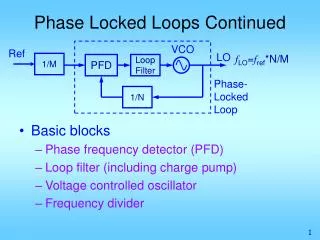
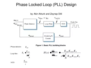
Components Of PLL • Phase Detector (PD):A nonlinear device whose output contains the phase difference between the two oscillating input signals. • Voltage controlled oscillator (VCO): Another nonlinear device which produces oscillations whose frequency is controlled by a lower frequency input voltage. • Loop filter
General sinusoid at reference input can be written as: Vin=Einsin(ωt)…….(1) • Assume VCO output signal is Vosc=Eoscsin(ωt- Ød+90) =Eosccos(ωot - Ød)……(2) • Phase Detector output: Vpd=KmVinVosc where Km is the multiplication constant
Vpd=KmEinEoscsin(ωt)cos(ωt-Ød) • Using the familiar trigonometric identity in terms of the PLL: Vpd=0.5KmEinEosc[sin(Ød) + sin(2ωt-Ød)] • The output of the low pass filter : Vcntl=0.5KlpKmEinEoscsin(Ød) For small Ød Vcntl=0.5KlpKmEinEoscØd
Capture Range: • The maximum difference between the input signals frequency and oscillators free running frequency where lock can eventually be attained is defined as the capture range. • The Phenomenon of “Beating”.
Lock Range: • The maximum frequency excursions over which the output remains locked with the input is called the lock range. • The maximum output of the low pass filter is given by Vcntl-max=0.5 KlpKmEinEosc when Ød=90. Therefore lock range is given by ωlck=KoscVcntl-max.
Types Of PLLs • Analog or Linear PLL (LPLL) • Digital PLL (DPLL) • All digital PLL (ADPLL)
LPLL • The LPLL (Best) or analog PLL is the classical form of PLL. All components in the LPLL operate in the continuous-time domain.
The phase detector is typically some form of analog multiplier. • The phase error function is of the form φ(t) = KmK1Asin [θ(t) − θ^(t)] ≈ KD[θ(t) − θ^(t)] • The loop filter may be active or passive, but it typically results in the loop being either first-order or second-order. • The design/analysis of the loop filter makes use of the Laplace transform.
DPLL The digital PLL is just an analog PLL with a digital phase detector. • The DPLL is a hybrid system • The DPLL is very popular in synthesizer applications
In the below figure the optional digital divider, and variations on it, are used in frequency synthesis applications.
Popular types of digital phase detectors include: – Exclusive or gate (EXOR) – Edge-triggered JK-flip flop – Phase frequency detector (PFD)
ADPLL • The all-digital PLL (classical all-digital) is distinctly different from the other two PLLs • The ADPLL is a digital loop in two senses: – All digital components – All digital (discrete-time) signals • There are many ADPLL building blocks, and many variations on putting them together.
ADPLL • The VCO is replaced by a Digitally Controlled Oscillator (DCO) or also called a Numerically Controlled Oscillator (NCO)
Phase Detector • A phase detector is a circuit that normally has an output voltage with an average value proportional to the phase difference between the input signal and output of VCO. Vpd=Kp∆Ф • Phase detectors can be a simple EX-OR gate, a sample and hold, an analog multiplier or a combination of D-flip flops.
XOR • The simplest phase detector is xor
An exclusive OR gate gives a high output when the signals are of opposite sign and a low output when they are of the same sign.
Phase Frequency Detector • It is a combination of tri state phase frequency detector and a charge pump.
Sample and Hold Phase Detector • A sample and hold circuit samples an input signal and holds on to its last sampled value until the input is sampled again.
EXCLUSIVE OR GATE VCC 4 0 5V VINA 1 0 PULSE(0V 5V 0US 0.1US 0.1US 2US 5US) VINB 9 0 PULSE(0V 5V 0US 0.1US 0.1US 3US 5US) RBA 4 3 4K RBB 4 8 4K RCSA 4 5 1.9K RCSB 4 11 1.9K RSDA 7 0 1.2K RSDB 12 0 1.2K RCX 4 14 3K RC 4 15 1.6K RCP 4 16 120 RX 18 0 1K DCA 0 1 DIODE DCB 0 9 DIODE DSA 5 6 DIODE DSB 11 13 DIODE DX 17 19 DIODE Q1A 2 3 1 QM Q1B 10 8 9 QM QS2A 5 2 7 QM QS2B 11 10 12 QM QSDA 6 7 0 QM QSDB 13 12 0 QM QX1 14 13 6 QM QX2 14 6 13 QM QS 15 14 18 QM QP 16 15 17 QM QO 19 18 0 QM .MODEL DIODE D (RS=40 TT=0.1NS) .MODEL QM NPN (IS=1E-14 BF=50 BR=1 RB=70 RC=4 TF=0.1NS TR=1NS) .TRAN 0.1US 15US .PLOT V(1) V(9) V(19) .END
Voltage Controlled Oscillators (VCOs) • The function of a VCO is to generate a stable and periodic waveform whose frequency can be varied with the applied control voltage. • The actual clock from PLL is the VCO output. • VCO’s frequency is modulated by the input voltage
Classification of VCO Depending on the type of output waveform, VCOs are classified as • Harmonic Oscillators • Relaxation Oscillators
Some of the commonly used VCOs-Ring Oscillators:Common in monolithic topologies and it uses odd number of inverters connected in feedback loop.-Other forms of VCOs, such as crytal oscillators and resonant oscillators essentially run on the same principle
VCO Circuit Design: • A simple design of VCO consists of a collector coupled astable multivibrator using n-p-n transistor with a control voltage. Step 1
*Voltage controlled Oscillator VCC 6 0 DC 5V VI 7 0 PULSE(0 5 0US 30US 30US 30US 40US) RC1 6 1 1K RC2 6 2 1K RE1 7 10 1K RE2 7 11 1K R3 7 8 2K R4 7 9 2K R5 8 0 4.7K R6 9 0 4.7K C1 1 4 150PF C2 2 3 150PF Q1 1 3 0 QM Q2 2 4 0 QM .MODEL QM NPN (IS=2E-16 BF=50 BR=1 RB=5 RC=1 RE=0 TF=0.2NS TR=5NS) Q3 3 8 10 QM1 Q4 4 9 11 QM1 .MODEL QM1 PNP (IS=2E-16 BF=100 BR=1 RB=5 RC=1 RE=0 TF=0.2NS TR=5NS) .IC V(1)=0 V(3)=0 .TRAN 0.1US 90US .PLOT TRAN V(2) V(7) .END
Loop filter: • The loop filter may be active or passive, but it typically results. • In the loop being either first-order or second-order. • A 1st order filter having a low frequency pole and high frequency zero is recommended. • Loop filter system functions, F(s), include: Filter Type Filter F(s) perfect integrator 1+sτ2/sτ1 imperfect integrator 1+sτ2/1+sτ1 lag or low pass 1/1+sτ
Filter Design • Design circuit is a simple RC low-pass filter which can extract the average value from the output of the phase detector. • This average value is used to drive the VCO R1 out in C1 Hlp(s)=1+sR2C1/1+s(R1+R2)C1 R2
low pass filter R1 1 2 86K C1 2 3 5PF R2 3 0 2K VIN 1 0 PULSE(0V 9V 0US 0US 0US 2US 5US) .TRAN 0.01US 15US .PLOT TRAN V(2) V(1) .END
The earliest widespread use of PLLs was for the horizontal and • vertical sweeps used in televisions. • PLLs were critical to development of color televisions also. • PLLs today: • –Cell phones, televisions, radios, pagers, computers, all • telephony, • – At low end: all software PLLs implement entire PLL functionality • on sampled data. • – At high end: optical PLLs used in clock recovery for 160 Gbps • data
Phase-locked loops are widely used for synchronization purposes • Space communications for coherent carrier tracking • and threshold extension • Bit and symbol synchronization • They are also used for: • Demodulation of frequency modulated signals • To synthesize new frequencies which are multiples of a • reference frequency, with the same stability as the • reference frequency.
Deskewing • the clock must be received and amplified • finite delay dependent on process,temperature and voltage between detected clock edge and the received data • delay limits the frequency at which data can be sent • deskew PLL on the receiver side phase-matches the clock at each data flip-flop to the received clock. • 2. Clock generation • multiplies lower-frequency reference clock (usually 50 or 100 MHz) up to the operating frequency of the processor that operate at Gigahertz
3. Spread spectrum • All electronic systems emit some unwanted radio • frequency energy • limits on this emitted energy and any interference • caused • spreading the energy over a larger portion of the • spectrum • 4. Jitter and noise reduction • reference and feedback clock edges can be brought into very • close alignment • phase and frequency of generated clock is unaffected by rapid • changes in voltages of the power supply lines and of the • substrate on which the PLL circuits are fabricated
1. Carrier Recovery • General block diagram of frequency recovery from a modulated signal. • When carrier has strong component in signal spectrum, PLL can lock. • When carrier is missing from signal spectrum, PLL must be preceded by a nonlinear element.
2. Costas Loop • A Costas loop can both recover the carrier and demodulate the data from a • signal. • If there were no modulation, the upper arm is simply a PLL lock to a carrier. • The effect of the lower arm of the loop is to lock to the modulation and cancel it • out of the upper arm of the loop. • Does the same thing as squaring loop, but down converts signal to baseband & • does filtering there.