MOS Current Mirror
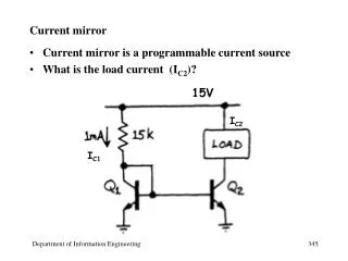
MOS Current Mirror. Section 9.2 J. Ou. A Simple Current Mirror. Example 1. Example #2. Trade-Offs in Current Mirror Design. Output resistance (1/gds) CDS W/L Current. I OUT =100 uA. For Same IOUT, L↓→W↓→GDS↑(Ro↓) →CDS ↓. Drop in Ro is not desired.

MOS Current Mirror
E N D
Presentation Transcript
MOS Current Mirror Section 9.2 J. Ou
Trade-Offs in Current Mirror Design • Output resistance (1/gds) • CDS • W/L • Current
IOUT=100 uA For Same IOUT, L↓→W↓→GDS↑(Ro↓) →CDS ↓ Drop in Ro is not desired.
Use Cascode to Increase output Resistance Rout is approximately gm3ro3ro2 L1=L2, but L3 need not equal to L2. Design Criteria: Choose Vb so that VY and VX. We will learn how to generate Vb in the next class.
Design Example VDS of T4 is not matched to VDS of T5. T4 has VDS of 999.1 mV. How come? Answer: VSD=0.2 was used as design criteria for T0 and T2.We need a transistor to absorb the difference between VDS of T4 (which is 0.6 V) and VSD of T2 (which is 0.2V) Bias I: 100 nA
Add More VGS to Minimize Difference in VDS VDS5=161.2 mV gives 50 nA VDS4 is 155.7 mV, provides 49.82nA.
Need for a Cascode T1 is designed to have a VSD of 0.4, leading to Vout=0.6 V. T3 is designed to have VDS of 200 mV, but it must sustain Vout=0.6 V. So we need to add a transistor to absorb the difference in V.