Current mirror
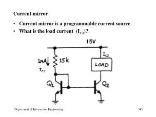
Current mirror. Current mirror is a programmable current source What is the load current (I C2 )?. 15 V. I C2. I C1. Twin - matched pair. Q1 and Q2 are matched pair (TWIN)

Current mirror
E N D
Presentation Transcript
Current mirror • Current mirror is a programmable current source • What is the load current (IC2)? 15V IC2 IC1
Twin - matched pair • Q1 and Q2 are matched pair (TWIN) • they have exactly the same performance because they are fabricated on the same chip, at the same temperature and have the same level of doping • Since Q1 and Q2 are matched, and have the same VBE • IC2 = IC1 • We can use the resistor in Q1 to control IC2 • IC2 = IC1 = (15V - 0.6V) / 15kW ~ 1mA
Current mirror with ratios other than 1:1 • Quiz: What is the current ratio? Why?
Current mirror with ratios other than 1:1 • Quiz: What is the current ratio? Why?
Temperature effects • IC increase with the temperature • if VBE remains constant, • IC grows at about 9% / oC • if IC remains constant, • VBE falls at 2mV / oC • a smaller VBE is enough to provide the same IC because of the higher temperature
Temperature effects • The great thing about mirror is that IC2 is not affected by temperature change ! • If we heat up Q1, will IC1 be changed? • VBE can only vary from 0.5 to 0.8V • IC remains more or less fixed at 1mA
Negative feedback • A deeper reason why IC1 is constant • temperature => IC1 • IC1 => voltage drop across 15k resistor => VBE1 => IC1 • This feedback mechanism keeps IC1 constant
Temperature compensation for amplifier • If VBE is fixed, what would happen if we heat up the transistors in the following circuits?
Auto-bias with feedback • Left-hand circuit (without feedback resistor RE) • extremely sensitive to temperature change • IC at a rate of 9%/oC, bias changed • Right-hand circuit (with feedback resistor RE) • temp , IC , VE , VBE (as VB is fixed), • sqeezing VBE so that IC • Another reason why IC is constant
The price to pay • lower gain ( = -RC/RE) in exchange for stability • Can we have both stability (constant DC bias) and high (ac) gain? • Yes !!
Requirements of output driver • High current output • need large current to drive the mechanical voice coil of the speaker’s driver • Voltage gain is not important • because signal has already been amplified • An emitter follower is perfect • VIN = VOUT • small current in (IB), large current out (IE) • Power out > power in => a power amplifier
Output driver circuit • A driver that produces large current over range +/-15V
Output driver circuit • Q1 and Q2 are both emitter followers • What is the use of the current source in Q1? • To replace RE • Problem with RE • If RE is too small => small input impedance • If RE is too large => small IC => small output impedance • Active load (the current source) • it has impedance => large input impedance • You choose large IC so that output impedance is small
Use a constant current source instead of resistor • Q2 is a power transistor, needs large base current • large resistor gives only small current • ideal constant current source has infinitely large impedance and can provide large current at the same time • Clever ! • Current source is an example of active load • Used extensively in integrated circuits because it is easier to fabricate transistors than resistors
Output driver circuit • DC offset voltage • 0.6V (the VBE) for a simple follower • Zero DC offset voltage in this circuit ! • Q1 (pnp) and Q2 (npn) are opposite type of transistors • Note the 0.6V voltage drops of VBE in Q1 and Q2 cancels each other out • So that 0V DC input gives 0V DC output
Current source and current sink • Current source • The ability of giving out current (flow out of the circuit) • Current sink • The ability of absorbing current (flow into the circuit) • Consider Q2 • Range of VE = +/- 15V • If VE > 0, current flowing out to load (source) • If VE < 0, current flowing in from load (sink)
Current source and current sink • Max source current (when Q2 is fully on) • If Q2 is fully ON (VCE=0) • max source current = 15V/8W ~ 2A • Max sink current (when Q2 is fully off) • IR = ISINK + IE • ISINK is max when IE = 0 (zero current from Q2) • this happens when VE= -15V • Max ISINK = 15 / 8 A
Max output power of the amplifier • Max output voltage swing • +/- 15V peak-to-peak • Average power dissipated on a 8W load =
Root-mean-square (RMS) voltage • Define RMS voltage as • Advantage • For ac voltage, the average power = • Hong Kong’s power supply : 240V • It is a RMS voltage
Quiescent (rest state, no signal) power dissipation • At rest state, 0V input gives 0V output • power dissipated in resistor = (0- -30)2/8 ~ 110W !! • power dissipated in transistor Q2 • quiescent collector current = 30V/8 = 3.75A • VCE= 15V, IC = 3.75A, • power= VCE IC = ~ 56W • total quiescent power dissipation = 110W+56W = 166W (HOT !!) • 14W amplifier gives out 166W heat (inefficient)
Push-pull emitter follower (Class B amplifier) • Problem with class A amplifier • quiescent power dissipation is many times larger than maximum output power • push-pull follower
Class B amplifier • Q1 (NPN) conducts on positive cycle • Q2 (PNP) conducts on negative cycle • 0V input, none of the transistor is conducting • No current, no power dissipation at Q1 and Q2 • No resistor, no power dissipation • Pros • Efficient, no wasted power • Cons • Cross-over distortion
Cross-over distortion • input have to be greater than 0.6V or less than -0.6V in order to make Q1 or Q2 conducting • Output = 0V when input is between +0.6V and -0.6V • Distortion
Class AB amplifier • Use diode to compensate for crossover distortion • R can be replaced by current source 0.6V
Amplifiers classification • Class A : transistors conduct all the time (360o) • Class B: transistors conduct only half of the time (180o) • Class AB: transistors conduct more than half of the time, and less than full time • Class C: transistors conduct less than half of the time
Differential Amplifier • A differential amplifier has two input terminals • only amplify the difference in signals • common signal is NOT amplified
Differential Amplifier • The pair of input signals can be separated into a common part and a differential part • e.g. (3V, 3.1V) inputs = (0.05V, -0.05V) (differential) (3.05V, 3.05V) (common) • Ideal differential amplifier • Large differential gain • Amplify the difference in signal • Zero common-mode gain • common signal produces zero output
DC Quiescent point • 0V input (because base is tied to ground) • VA ~ -0.6V • ITAIL = • ITAILis pretty constant because • large negative voltage (-15V) • variation of VA is small in practice • A simple constant current source • Can be improved by using a real current source • By symmetry (same VBE), IC on both transistors is about 1mA each
Differential gain • The key in understanding differential gain • feed a DVIN/2 signal on one input, and a -DVIN/2 on the other, VA does not move VA DVIN/2 -DVIN/2
Differential gain • Because VA is fixed, only need to analyze the part of the circuit above “A” • just a common emitter amplifier
Differential gain • Common emitter amplifier gain • VOUT/VIN = -RC/(RE+re) • In out case, input = -DVIN/2 • Differential gain
Common mode gain • Feed a common signal to both inputs, VA goes up • model the 7.5k tail by two 15k in parallel • I = 0 because of symmetry • split the circuit in two • Common mode gain • GCM= -RC/ (re+RE+2(RTAIL)) Vin
CMRR (Common-mode rejection ratio) • CMRR = differential gain / common mode gain • Ideal differential amp has • large differential gain • small common mode gain • Therefore CMRR should be as large as possible • RTAIL should be as large as possible
CMRR • Replace RTAILby constant current source • CMRR ~ 100,000:1 !! • 100dB ! • dB = 20log 105 = 20*5 = 100
How to generate composite signal in the lab • Composite signal = common-mode + differential signal • use function generator 1 to generate the common-mode signal (tied to true ground) • use function generator 2 to generate the differential signal (floating ground, ground is connected to the output of generator 1) • Make sure the ground of generator 2 is floating (not connected to the main supply)
Generator 2 Common signal Generator 1
Vdiff +Vcommon Floating ground ! Vcommon Vcommon (from gen 1)