The Devices
400 likes | 547 Views
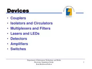
The Devices. Cross-section of. pn. -junction in an IC process. The Diode. B. A. Al. SiO. 2. p. n. A. Al. A. p. n. B. B. One-dimensional. representation. diode symbol. Depletion Region. Diode Current. Forward Bias. Reverse Bias. SPICE Parameters.

The Devices
E N D
Presentation Transcript
Cross-section of pn -junction in an IC process The Diode B A Al SiO 2 p n A Al A p n B B One-dimensional representation diode symbol
Carriers and Current • Carriers always flow from the Source to Drain • NMOS: Free electrons move from Source to Drain. • Current direction is from Drain to Source. • PMOS: Free holes move from Source to Drain. • Current direction is from Source to Drain.
IGFET • The dimension of SiO2 layer is about 0.02 to 0.1 micron. • Gate is isolated thus Insulated-Gate FET • Due to insulation the current flowing through the gate terminal is extremely small of the order of 10^-15 A. • Drain is always kept as more positive than the source. • The current flows from the Drain to Source • P-n junctions are kept under the reverse bias conditions • Typically the Length of the device is from 1 to 10 micron.
MOS Transistor structure • Polysilicon –Heavily doped noncrystalline silicon. • Polysilicon allows the dimensions of the transistor to be realized accurately. • Gate Oxide – Silicon dioxide. • Thickness of gate oxide – 7 to 20nm. • No d.c. through gate. • Normally, p substrate is connected to 0V in digital circuits and to negative voltage in analog circuits.
Symmetry The transistor is symmetric: The Drain (which is equivalent to a BJT’s Collector) and the Source (which is equivalent to a BJT’s Emitter) are fully symmetric and therefore interchangeable
All MOS p-n Junctions Unlike a BJT transistor, in which one of the p-n junctions is typically forwardly biased, and the other reversely biased, in a MOSFET all p-n junctions must always be kept reversely biased!
The MOSFET Channel • Under certain conditions, a thin channel can be formed right underneath the Silicon-Dioxide insulating layer, electrically connecting the Drain to the Source. The depth of the channel (and hence its resistance) can be controlled by the Gate’s voltage. The length of the channel (shown in the figures above as L) and the channel’s width W, are important design parameters.
REGION OF OPERATIONCASE-1 (No Gate Voltage) • Two diodes back to back exist in series. • One diode is formed by the pn junction between the n+ drain region and the p-type substrate • Second is formed by the pn junction between the n+ source region and the p-type substrate • These diodes prevent any flow of the current. • There exist a very high resistance.
REGION OF OPERATIONCreating a channel • Apply some positive voltage on the gate terminal. • This positive voltage pushes the holes downward in the substrate region. • This causes the electrons to accumulate under the gate terminal. • At the same time the positive voltage on the gate also attracts the electrons from the n+ region to accumulate under the gate terminal.
REGION OF OPERATIONCreating a channel • When sufficient electrons are accumulated under the gate an n-region is created, connecting the drain and the source • This causes the current to flow from the drain to source • The channel is formed by inverting the substrate surface from p to n, thus induced channel is also called as the inversion layer. • The voltage between gate and source called vgs at which there are sufficient electron under the gate to form a conducting channel is called threshold voltage Vth.
MOS Transistor Current direction • The source terminal of an n-channel(p-channel) transistor is defined as whichever of the two terminals has a lower(higher) voltage. • When a transistor is turned ON, current flows from the drain to source in an n-channel device and from source to drain in a p-channel transistor. • In both cases, the actual carriers travel from the source to drain. • The current directions are different because n-channel carriers are negative, whereas p-channel carriers are positive.
MOS I/V For a NMOS, a necessary condition for the channel to exist is:
REGION OF OPERATIONApplying small Vds • Now we applying some small voltage between source and drain say 0.3V. • The voltage Vds causes a current to flow from drain to gate. • Now as we increase the gate voltage, more current will flow. • Increasing the gate voltage above the threshold voltage enhances the channel, hence this mode is called as enhancement mode operation.
MOSFET Current-Voltage Relationships • The DC gate current is always zero: IG = 0 • Therefore, when a channel is created, the drain current equals the source current: ID =IS
MOS Transistor - Symbols pMOS Transistor nMOS Transistor
Operation – nMOS Transistor • Accumulation Mode - If Vgs < 0, then an electric field is established across the substrate. • Depletion Mode -If 0<Vgs< Vtn, the region under gate will be depleted of charges. • Inversion Mode – If Vgs > Vtn, the region below the gate will be inverted.