Atomic Layer Deposition for SCRF
Atomic Layer Deposition for SCRF. J. Norem ANL/HEP. RF in the MTA 11/15/10. Atomic Layer Deposition. Atomic Layer by Layer Synthesis Method similar to MOCVD Used Industrially Semiconductor Manufacture for “high K” gate dielectrics “Abrupt” oxide layer interfaces

Atomic Layer Deposition for SCRF
E N D
Presentation Transcript
Atomic Layer Deposition for SCRF J. Norem ANL/HEP RF in the MTA 11/15/10
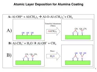
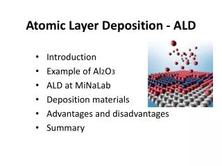
Atomic Layer Deposition • Atomic Layer by Layer Synthesis Method similar to MOCVD • Used Industrially • Semiconductor Manufacture for “high K” gate dielectrics • “Abrupt” oxide layer interfaces • Pinhole free at 1 nm film thicknesses • Conformal, flat films with precise thickness control • Electroluminescent displays • No line of sight requirement • Large area parallel deposition • Parallel film growth technique; Inside of large tubes can be done at once.
Ellipsometry Atomic Force Microscopy 4000 3500 3000 2500 Thickness (Å) 2000 1500 1000 Seagate, Stephen Ferro 500 0 • RMS Roughness = 4 Å (3000 Cycles) • ALD Films Flat, Pinhole free 0 500 1000 1500 2000 2500 3000 Flat, Pinhole-Free Film AB Cycles • Film growth is linear with AB Cycles ALD Reaction Scheme • ALD involves the use of a pair of reagents. • each reacts with the surface completely • each will not react with itself • This setup eliminates line of site requirments • Application of this AB Scheme • Reforms the surface • Adds precisely 1 monolayer • Pulsed Valves allow atomic layer precision in growth • Viscous flow (~1 torr) allows rapid growth • ~1 mm / 1-4 hours • No uniform line of sight requirement! • Errors do not accumulate with film thickness. • Fast! ( mm’s in 1-3 hrs ) and parallel • Pinholes seem to be removed. • Bulk
Apparatus • Hot wall reactor (RT-400 C) • Always coat the wall – now it will be useful
Oxide Nitride Element Ph/As C F S/Se/Te Demonstrated ALD A/B Reactions Element
150 nm Aerogels coated with W • Conformal Coating and “sharp” points • Aerogels are low density nanoporous materials consisting of bundles of nm scale filaments • ALD can be used to deposit W metal atomic layer by layer on this filaments Overall Reaction: WF6 + Si2H6 → W + products 10 nm filaments
3 c W 7 c W 80 nm 80 nm Microscopy of W-Coated Carbon Aerogels SEM TEM • Aerogel filament diameter increases with ALD W Cycles
Higher-TcSC: NbN, Nb3Sn, etc Nb, Pb Insulating layers Goal of ALD SCRF • Build “nanolaminates” of superconducting materials • ~ 10- 30 nm layer thicknesses
Conclusions • ALD is an intriguing synthesis technique with many useful properties • Conformal coating means increased radius of curvature • Parallel (non-line of sight) method • Flat samples directly map to complex shape samples even with high aspect ratios • Layer by layer growth on complex shapes • Useful for higher field gradients in SRF and NCRF