Download
1 / 33
330 likes | 375 Views
Scale-Up Activities in Atomic Layer Deposition at Argonne. Jeffrey Elam, Anil Mane, Joe Libera December 9, 2011. Large Area Picosecond Photodetector Collaboration Meeting December 9-10, 2011, Argonne National Laboratory. Outline. Introduction to ALD (1 slide) ALD on 33mm plates

E N D
Scale-Up Activitiesin Atomic Layer Deposition at Argonne Jeffrey Elam, Anil Mane, Joe Libera December 9, 2011 Large Area Picosecond Photodetector Collaboration Meeting December 9-10, 2011, Argonne National Laboratory
Outline Introduction to ALD (1 slide) ALD on 33mm plates Challenges with scale-up to larger substrates Conclusions
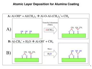
CH4 CH3 CH3 CH3 CH3 Al Al Al Al CH3 CH3 CH3 CH3 CH3 CH3 CH3 CH3 CH3 CH3 CH3 CH3 CH3 CH3 CH3 Al Al Al Al OH OH OH OH OH OH OH OH OH OH OH OH OH CH4 H2O H2O OH OH CH3 CH3 Al Al Binary Reaction Sequence for Al2O3 ALD Trimethyl Aluminum (TMA) A) Al(CH3)3 B) H2O • 1 ALD Cycle of TMA/H2O Deposits 1 Al2O3 “Monolayer”
Multiple 33mm MCPs in Tubular ALD Reactor Chem-2 Resistive Coating • Thickness uniformity on monitor Si(100) <2% • The resistive layer thickness ~800A • Similar thickness trend observed on second batch of 5 MCPs • Excellent batch-to-batch reproducibility
Resistance Comparison for 9 MCPs (air vs. vacuum) Chem-2 Resistive Coating • Average resistance (2 batches of 5 plates) • 115 ±12 M ~10% resistance variation
Challenges to Coating Larger Areas Need a bigger reactor Non-ideal ALD surface reactions High aspect ratios High surface areas
Large Substrate Reactor 12x18” box 2” tube From 1x1-in plates to 12-in x 18-in plates
Coating 8” MCPs in Beneq 300 mm chamber
Non-Ideal ALD Surface Reactions In2O3 ALD in Large Substrate Reactor InCp + O3→In2O3 • In2O3 films were thinner downstream in reactor • Indium oxide catalyzes ozone destruction In2O3 • O3 O* + O2
Scale-up of ALD In2O3 to 12”x18” Substrates InCp + H2O + O2 InCp + O3 • Thickness deviation: 2.5% • Resistivity deviation: 6% • Thickness deviation: 45% • Non-self limiting ALD reactions can lead to non-uniform films in larger ALD systems
Coating High Aspect Ratios: ALD W in Anodic Alumina 15 μm 40 nm pores, 70 microns long • Conformal coating on all exposed surfaces • Aspect ratio ~ 1000
Large Substrate Surface Area: Silica Gel Powder • 100 micron particles, 30 nm pores (aspect ratio ~ 2000) • Surface area = 100 m2/g • Powder bed fixture for ~1 g support
Self-Limiting Al2O3 ALD Planar Surface Silica Gel • Self-limiting growth on planar and porous surfaces • Exposures increased by x100
Surface Areas of Glass Capillary Arrays: (thanks Jason M.) Empty tube reactor: ~2000cm2 Empty LSR: ~4000 cm2 Empty Beneq 300mm: ~1600 cm2 • MCP aspect ratio = 60 (we’ve done 10^5) • 8” MCP surface area = 6.5 m2 (we’ve done 10^3) • Piece of cake…
Work Plan 1) Qualify Beneq for Chem2 coatings using coupons and 33mm MCPs in new 300mm chamber 300 mm chamber 200 mm chamber 2) Coat single 8”x8” MCPs in 300 mm chamber 3) Coat multiple (1-4) 8”x8” MCPs in 300 mm chamber X) Coat multiple (20) 8”x8” MCPs in 3D chamber
Al2O3 ALD in 300 mm Reactor <1% non-uniformity in 100 nm coating Works great!
Chem-2 ALD in 300 mm Reactor Precursor inlet direction • Test Metrics: • Optimized chemistry -2 baseline process on 300mm chamber: • Deposit 300mm wafer at same condition as MCP deposition. • Evaluated the resistivity uniformity across the large area 5 6 7 8 9 10 11 12 13 14 15 16 17 18 19 20 21 22 23 24 25 26 1 2 3 4 300mm
Resistivity of Chem2 coating at different locations on 300mm wafer Works great for Chem-2!
Chem-2 thickness NU on 300mm wafer with 8”x8” MCP on top:2D thickness map 1-sigma thickness: 10% 300mm August 22, 2011 • We may need square chamber? 300mm
8” 40µm MCP Pair Gain Map (thanks Ossy, Jason, SSL) Y gain slice Y gain slice X gain slice FIRST Gain map – Looks awful - multifiber visible, lots of gain non-uniformity This is from the thickness non-uniformity
Troubleshooting in Beneq reactor wall 300 mm wafer 8” MCP Side View assumed flow distribution Top View • ALD conductive coating with MCP substrate installed over Si(100) 300 mm wafer • Measure film thickness on Si wafer using 4-point probe conductivity (easy, quantitative)
Process testing on 8” MCP on Beneq • Baseline process: 50 cycles conductive coating (No MCP) Precursor inlet 1-sigma = 4%
Thickness values form resistance and 2D map: 1-sigma = 4% 57% 52% 10% 24% Tested many ideas, hardware, software, reactor breaks, etc. (3 months)
Troubleshooting in Beneq: Al2O3 Side View • ALD Al2O3 coating with MCP substrate installed over Si(100) 300 mm wafer • Visually assess coating uniformity • Measure film thickness on Si using ellipsometry
Troubleshooting in Beneq: Al2O3 Precursor inlet 50 nm 100 nm 150 nm Anil: “We have a flow problem… we need a square chamber”
Troubleshooting in Tubular Reactor 2cm x 30 cm Si(100) substrate, rest 2x20cm MCP 2 mm above Si 500 cycles TMA/H2O for Al2O3 2 inches MCP Si • Narrow gap under MCP • High surface area 26
Troubleshooting in Tubular Reactor 2-5-2-5, 0.05 Torr doses 2-5-2-5, 0.2 Torr doses 2-5-2-5, 1 Torr doses • Some non-uniformity, not as bad as Beneq
Troubleshooting in Tubular Reactor Si MCP Si • Narrow gap under MCP • Narrow gap over MCP • High surface area
Troubleshooting in Tubular Reactor 2-5-2-5, 0.05 Torr doses • Same bad non-uniformity as in the Beneq
Troubleshooting in Tubular Reactor • Narrow gap under MCP” • Narrow gap over MCP • No high surface area Si Si 2-5-2-5, 0.05 Torr doses • Nearly perfect uniformity
What is going wrong in Beneq? reactor wall • Narrow gap under MCP • Narrow gap over MCP • High surface area 300 mm wafer 8” MCP Side View actual flow distribution Top View • No flow in the gap • Slow outgassing/diffusion from MCP • Precursors mix, CVD
What is going wrong in Beneq? Precursor inlet 50 nm • The problem: flow is bypassing the MCP • Solution: we need to confine the flow so that it is forced to pass in the gap between the plate(s) and the reactor wall. • We have a flow problem… we need a square reactor. 100 nm 150 nm
Potential Solution, Conclusions reactor wall 300 mm wafer 8” MCP Side View Top View • Equal gap • Convert circle into square • CFD modeling would be helpful • Listen to Anil