Atomic Layer Deposition
Atomic Layer Deposition. ENMA465 14 May 2003. Nicole Harrison Bryan Sadowski Anne Samuel Kunal Thaker. Presentation Outline. ALD Theory and Processes Applications Focus on ALD applications in gate dielectrics Equipment Comparisons to other Processes Current and Future Development

Atomic Layer Deposition
E N D
Presentation Transcript
Atomic Layer Deposition ENMA465 14 May 2003 Nicole Harrison Bryan Sadowski Anne Samuel Kunal Thaker
Presentation Outline • ALD Theory and Processes • Applications • Focus on ALD applications in gate dielectrics • Equipment • Comparisons to other Processes • Current and Future Development • Questions
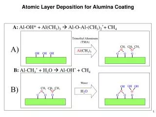
What is ALD? • ALD (Atomic layer deposition) previously known by the name ALE (Atomic layer Epitaxy) was originated by T.Suntola in Finland. • Deposition method by which precursor gases or vapors are alternately pulsed on to the substrate surface. • Precursor gases introduced on to the substrate surface will chemisorb or surface reaction takes place at the surface.
ALD • Surface reactions on ALD are all self-limiting. • Self-limiting characteristics of the process steps is the foundation of ALD. • Two fundamental self-limiting mechanisms in ALD: CS-ALD and RS-ALD. • CS-ALD: Chemisorption Saturation process followed by exchange reaction. • RS-ALD: Sequential surface chemical reaction.
CS-ALD Process • Substrate is exposed to the first molecular precursor. The first molecular precursor is retained on the surface by chemisorption. • Second precursor is introduced on to the surface, which reacts on the surface of the first precursor. • Exchange reaction takes place between the two precursors and by-products are formed. • Exchange reaction continues till the second precursor reacts with first precursor: self-limiting step. • Final reaction is ML2+AN2®MA(film) + 2 LN • Sequence is repeated to grow films.
RS-ALD Process • Promoted by chemistry between reactive surface and reactive molecular precursor. • Deposition process is as a result of the chemical reaction between reactive molecular precursors and substrate. • Substrate surface is made reactive by certain surface groups. And first precursor is introduced to this surface. • The reaction now looks like this AN + ML2® AML +NL(A) reaction self-saturates until AN groups are converted to AML groups.
RS-ALD Process • Followed by this reaction, the first precursor is removed by inert gas purging prior to the introduction of second precursor. • Second precursor is introduced, which reacts with ML surface to form AML + AN2® MAN + NL(B) • Self saturates • The surface now looks like initial surface (AN) and surface is now ready for reaction (A). The repetition of ABAB…sequence will deposit films. • During each half-reaction(A&B), surface functionality changes from one surface species to another.
ALD Precursor Requirements • Must be volatile and thermally stable • Preferrably liquids and gases • Can be solids • no sintering related problems • Should Chemi-sorb on surface or react agressively with surface groups and each other • Short saturation time, good deposition rate, no gas phase reactions • Should not self-decompose • Destorys self-limiting property • Affects thickness, uniformity, and containation • Should not etch, dissolute into film or substrate • Prevents self-limiting film growth • Examples of substrates • Zn, Cd, S, Se, metal halides like AlCl3, TiCl4,TaCl5, Alkyls, b-Diketonates etc [2].
Transistor Gate Dielectrics MEMS Opto-electronics Diffusion Barriers Flat- Panel displays Organic Light Emitting Diodes (OLED) Interconnect Barriers Interconnect seed layer DRAM and MRAM dielectrics Embedded capacitors All thin films (<90 nm) Electromagnetic recording heads Applications
Applications • Transistor gate dielectrics • Smaller transistor sizes • Smaller channel lengths • Thinner gate oxide (limit of ~2.3 nm) • Larger leakage current • Need for high-K dielectrics for transistor gate dielectrics • Will allow for the use of thicker gate dielectrics • Lower leakage current • Lower power loss
Applications • New processes are concurrently being developed as new materials are being tested • ALD provides one of the best alternatives for depositing these new materials • Conformality • Uniformity • Compositional Control • Thickness control
Equipment ● Closed System Chambers - The Reaction chamber walls are such that they effect the transport (trajectory, etc.) of the precursors. ● Open System Chambers - Dimensions of reaction chamber do not interfere with ALD process (very large relative to wafer position). ●Semi-Closed System chambers - A channel is used with the top and bottom surfaces consisting of two separate wafers and the precursor gas is passed through the center. ●Semi-Open System chambers - Similar to a semi-closed system except one side is a wafer and the other side is gas- limited.
Equipment • CVD conversion to ALD • The installation of a module: facilitates fast gas switching • ALD specific equipment • Wafer output • Reaction volume • Factory Automation • Consistency • Conformality • Uniformity
Equipment • Research into more efficient equipment design continues • PEALD/ ALD reactor developed by Genitech Corporation • ● Hf[N(CH3)2]4 as the reactant • species with an O2 plasma • and H2O • ● Temperature in the range of • 200-350C • ● Ar is the carrier and purge • gas • ● Allows for increase in the • choice of reactants • ● Better film quality • ● Increased deposition rates
Comparison of ALD to CVD and PVD • Process description • ALD • atomic layer-by-layer deposition process where precursor is introduced into system, allowed to react with substrate surface until saturation, remaining by-products or unreacted gases are purged, process is repeated to form a monolayer/film • CVD • chemical reaction between gaseous precursors in gas phase; solid product of reaction is deposited on surface of substrate. • PVD • deposition process in gas phase where source material is physically transferred in the vacuum to the substrate without any chemical reactions being involved
Comparison Continued • self-limiting: gas-surface reactions occur till surface is saturated • Precursors are introduced into system separately • reactions occur at the surface • precise thickness control • 100% step coverage even at high aspect ratios • Films are very uniform, smooth, and stoichiometric
Comparison Continued • less contamination • low pressures • typically less than 10-6 torr • Film thickness can be as low as 1nm • produces amorphous films • lower deposition temperatures • as low as 180oC for HfO2
Comparison Continued • slow deposition rates because have to form monolayer in two steps • HfO2: dep. rate of 0.1nm/s @ 300oC • Growth rate • increases, reaches a max, and decreases slightly as temperature is increased • increases with number of cycles Thin Solid Films, 427(1-2), p.147-151.
Current Developments • Materials being used • ZrO2 , Al2O3, HfO2 • All exhibit good qualities • thickness control • good conformity • excellent step coverage
Current Developments • High-k materials • traps electrons between barrier gate and SiO2 • prevents burrowing of electrons through SiO2 • High barrier height • energy required for electrons to pass from gate to SiO2 material formula kox silicon oxide SiO2 3.9 silicon nitride Si3N4 7 Oxynitrides SixNyOz 4 - 7 aluminum oxide Al2O3 9 tantalum pentoxide Ta2O5 25 hafnium oxide HfO2 30 - 40 zirconium oxide ZrO2 25 barium strontium titanate (BST) BaSrTiO3 300
Future Developments • HfO2-Al2O3 laminate • Being Developed by Samsung • combines good qualities of both • Reduced current leakage • due to high-k of HfO2 and high barrier height of Al2O3
Future Developments • SiN/SiO2 stack gate-dielectric • SiO2 experiences soft-breakdown • due to differences in thermal expansion, high electric field, and strained Si-O bonds • low thermal budget (£550oC) • lower leakage current • higher reliability • soft-breakdown free • fewer wasted samples • Reduces Boron penetration in SiO2
Future Developments • Zr(t-OC4H9)4, commonly called ZTB being used to replace ZrCl4 as a precursor when making ZrO2 • Cl supposed to be purged once Zr has been reacted • sometimes reacts with substrate • can cause damage to whole system
References • Leskela Markku, Ritala Mikko. " Atomic Layer Deposition (ALD): From Precursors to Thin Film Structures". Thin Solid films, 2002 Vol 409. PP 138-139. • Ritala Mikko. "Fundamentals of ALD Chemistry" presented at AVS Topical Conference on Atomic layer deposition, May 14-15. 2001 Monterey, California. • Sneh Ofer, Phelps Robert et.al. “ Thin film atomiclayer deposition equipment for semiconductor processing” . Thin solid films, 2001 Vol 402. PP 248-261. • Scott Thompson, Portland Technology Development, Intel Corp. Paul Packan, Technology Computer Aided Design, Intel Corp. Mark Sohr, Portland Technology Development, Intel Corp. Intel Technology Journal. MOS Scaling: Transistor Challenges for the 21st Century. 10 April 2003.<http://www.intel.com/technology/itj/q31998/articles/art_3.htm>. • Ho-Kyu Kang. Samsung Electronics Co., LTD. ALD high k materials for gate and capacitor gate dielectrics. ALD Conference 2002. • ASM. The process of innovation. Pulsar. Single Wafer Atomic Layer CVD. 10 April 20003. <http://www.asm.com/prod_pulsar.asp>. • Moo-Han Corporation. ALD System. ELFRA 7000 Series. 10 April 2003.<http://www.moo-han.com/eng/html/product_ald_2.html>. • Dae-Youn Kim, Kyung-Il Hong, Jeongseok Ha, Cheol-Min Chang, Seung-Woo Choi, Hyung-Sang, Park, Yong-Min Yoo, Wonyong Koh and Choon-Soo Lee.Plasma Enhanced Atomic Layer Deposition of HfO2.Genitech, Inc. ALD Conference 2002. • Ho-Kyu Kang, Samsung Electronics Co., LTD, San#24 Nongseo-Ri, Giheung-Eup, Yongin-City, Gyeonggi-Do, Korea 449-711 • Anri Nakajima and Shin Yokoyama, Research Center for Nanodevices and Systems, Hiroshima University 1-4-2 Kagamiyama, Higashi-, Hiroshima, Hiroshima 739-8527, Japan

