Download
1 / 9
100 likes | 254 Views
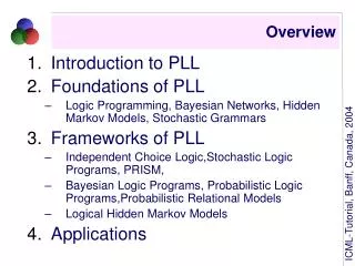
Learn about Phase Locked Loop design with detailed insights into Phase Detector, Loop Filter, VCO, and more. Explore schematics, current pumps, and simulation results for a deeper understanding.

E N D
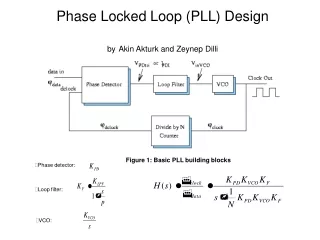
Phase detector: • Loop filter: • VCO: Phase Locked Loop (PLL) DesignbyAkin Akturk and Zeynep Dilli Figure 1: Basic PLL building blocks
Phase Detector Design Figure 2: Phase Frequency Detector and the Loop Filter Figure 3: PD and Loop Filter responses to input transients
Voltage Controlled Oscillator Figure 4: The schematics of the VCO Figure 5: Schematics of the Current Pumps
Design Considerations for the VCO Figure 6: I-Vin for Current Pumps Figure 7: Vin-fosc Relation
Ripple Carry Counter Figure 8: The Schematics of the 10-Bit Input Counter
PLL Building Blocks and Design Considerations Revisited Figure 8: Overall PLL Schematics
Pspice Simulation Result I Figure 10: Reference Clock and the Output of the Counter
Pspice Simulation Result II Figure 11: Loop Filter and VCO Inputs
Pspice Simulation Result III Figure 12: VCO Output at the Start and the End of the Simulation