Download
1 / 53
540 likes | 927 Views
Properties of GaN Films Grown by Atomic Layer Deposition Using Low-temperature III-nitride Interlayers J. R. Gong Department of Materials Science and Engineering Feng Chia University June 4, 2004. Co-workers. C. L. Wang B. H. Shih Y. L. Tsai I. H. Chien

E N D
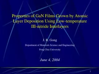
Properties of GaN Films Grown by Atomic Layer Deposition Using Low-temperature III-nitride Interlayers J. R. Gong Department of Materials Science and Engineering Feng Chia University June 4, 2004
Co-workers C. L. Wang B. H. Shih Y. L. Tsai I. H. Chien W. T. Liao S. W. Lin
OUTLINE Applications of III-nitrides • Fundamental aspects of ALD • LT-III-nitride interlayers — LT-GaN interlayer — LT-AlN interlayer — Ternary LT-AlGaN interlayer • Conclusions
Elemental and compound semiconductors Column IV: Si, Ge, SiGe, SiC Column III and V: GaAs, InP, InAs, InSb, GaN and alloys Column II and VI: ZnSe, CdS, HgTe and alloys
Semiconductor bandgaps UV-wide bandgap (GaN, ZnSe) IR-narrow bandgap (InSb, HgTe) Direct (mostly III-V): light emission possible LEDs, Lasers Indirect (mostly Si): light emission forbidden transistors, ICs
UV region Bandgap engineering
Advantages of III-nitrides Direct band gap The adjustability of band gap from 1.9eV (InN) to 6.2eV (AlN) Good radiation hardness High temperature resistance
Applications of III-nitride devices HBLEDs — traffic signal — full-color outdoor display — back light for LCD LDs — DVDs High Power Electronics
LED traffic signal Reacting speed of LEDs is 20 times faster than traditional light bulbs.
LED Chip substrate
Photographs of the home-made ALD growth system
A schematic diagram of the ALD system for the growth of III-nitride films Hydrogen Purifier Susceptor TMG TMA R.F. Coil H 2 Quartz NH 3 N 2 Exhaust Three-way Mass Flow Valve Regulator Valve Controller
A schematic diagram of the rotating susceptor for ALD process
Fundamental aspect of atomic layer deposition (ALD) (A) (B) AX AX AB(sub.) AB(sub.) (C) (D) BY AB (monolayer) AB(sub.) AB(sub.) • An ideal ALE growth cycle produces a monolayer AB compound.
Influence of low temperature GaN intermediate layers on the properties of GaN films
HT: 1000 ℃ 150, 380, 600 nm A schematic structure of HT-GaN films without LT-GaN interlayer
(a) (b) (c) SEM micrographs of the surface morphologies of HT-GaN films grown on (0001) sapphire substrates 150 nm 380 nm 600 nm
HT: 1000 ℃ LT: 500 ℃ (a) (b) (c) (d) Schematics of HT-GaN films inserted with LT-GaN interlayers
(a) (b) (c) (d) SEM surface morphologies of HT-GaN films inserted with a LT-GaN interlayer 7 nm 0 nm 20 nm 70 nm
The arrangement of Ga adatoms is merited by the suppression of surface kinetics at low growth temperatures, which is believed to stop the extension of mosaic structure from the underlying 150 nm-thick HT-GaN film during the growth of LT-GaN interlayer. A LT-GaN interlayer thickness deviated away from its optimised value was observed to deteriorate the quality of the subsequently grown HT-GaN film. The role of LT-GaN interlayer on the growth of HT-GaN film
RT PL spectra of HT-GaN films inserted with different LT-GaN interlayer thicknesses (The inset shows the effect of interlayer thickness on the PL emission energy)
(0002) DCXRD curve of a HT-GaN film inserted with a 20-nm-thick LT-GaN interlayer
Cross-sectional TEM image of a HT-GaN film inserted with a 20-nm-thick LT-GaN interlayer
A schematic structure of GaN films having various LT-GaN interlayer thicknesses HT-GaN 0.9 m LT-GaN 25Å<d<300Å HT-GaN 0.6 m AlN buffer sapphire
RT PL spectra of GaN films inserted with LT-GaN interlayers having different thicknesses
PL linewidth of GaN films inserted with LT-GaN interlayers having various thicknesses
Influence of low temperature AlN intermediate layers on the properties of GaN films
A schematic structure of GaN films having various LT-AlN interlayer thicknesses HT-GaN 0.9 m LT-AlN interlayer 25Å<d<125Å HT-GaN 0.6 m AlN buffer sapphire
RT PL spectra of GaN films inserted with AlN interlayers having different thicknesses
PL linewidth of GaN films inserted with LT-AlN interlayers having various thicknesses
Influence of low temperature AlGaN intermediate layers on the properties of GaN films
A schematic structure of GaN films having various LT-AlxGa1-xN interlayer thicknesses HT-GaN 0.9 m LT-AlxGa1-xN 25Å~200Å HT-GaN 0.6 m AlN buffer sapphire
RT PL spectra of GaN films having 2.5 nm-thick LT-AlGaN interlayers with different Al contents
RT PL spectra of GaN films having 5 nm-thick LT-AlGaN interlayers with different Al contents
RT PL spectra of GaN films having 7.5 nm-thick LT-AlGaN interlayers with different Al contents
RT PL spectra of GaN films having 10 nm-thick LT-AlGaN interlayers with different Al contents
PL linewidth of the GaN films versus the Al content of the 2.5 nm-thick LT-AlGaN interlayer
PL linewidth of the GaN films versus the Al content of the 5nm thick LT-AlGaN interlayer
PL linewidth of the GaN films versus the Al content of the 7.5nm thick LT-AlGaN interlayer
PL linewidth of the GaN films versus the Al content of the 10nm thick LT-AlGaN interlayer
RT PL spectra of GaN films inserted with different Al0.6Ga0.4N interlayers thicknesses
PL linewidth of GaN films inserted with LT-Al0.6Ga0.4N interlayers having various thicknesses