Download
1 / 23
250 likes | 513 Views
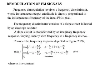
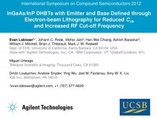
International Symposium on Compound Semiconductors 2012. InGaAs/InP DHBTs with Emitter and Base Defined through Electron-beam Lithography for Reduced C cb and Increased RF Cut-off Frequency.

E N D
International Symposium on Compound Semiconductors 2012 InGaAs/InP DHBTs with Emitter and Base Defined through Electron-beam Lithography for Reduced Ccb and Increased RF Cut-off Frequency Evan Lobisser1,*,Johann C. Rode, VibhorJain2, Han-Wei Chiang, AshishBaraskar3, William J. Mitchell, Brian J. Thibeault, Mark J. W. Rodwell Dept. of ECE, University of California, Santa Barbara, CA 93106, USA (Now with 1Agilent Technologies, Inc., CA, 2IBM Corporation, VT, 3GlobalFoundries, NY) Miguel Urteaga Teledyne Scientific & Imaging, Thousand Oaks, CA 91360 Dmitri Loubychev, Andrew Snyder, Ying Wu, Joel M. Fastenau, Amy W. K. Liu IQE Inc., Bethlehem, PA 18015 *evan.lobisser@agilent.com, +1 (707) 577-5629
Outline • Motivation • HBT Design & Scaling • Fabrication Process & Challenge • Electrical Measurements • Conclusion 2
Why THz Transistors? Digital logic for optical fiber circuits 0.3- 3 THz imaging systems THz amplifiers for imaging, communications 0.1-1 Tb/s optical fiber links High gain at microwave frequencies: Precision analog design, high resolution ADCs, DACs 3
Type-I InP DHBTs at UCSB Emitter: n++InGaAs cap n InP XX’: z Base: p++InGaAs Doping grade Drift collector: n-InGaAs/InAlAs grade n-InP Sub-collector: n++InGaAs cap n++InP Semi-insulating InP substrate C E B X’ Collector BP CP Emitter Base X z 4
HBT Scaling Laws To double bandwidth of a mesa DHBT: Keep constant all resistances and currents Reduce 2:1 all capacitances and transport delays Epitaxial scaling Lateral scaling Surface prep & doping Keep lengths the same, reduce widths 4:1 for thermal considerations 5
Epitaxial Design Vbe = 1.0V, Vcb = 0.5V, Je = 0, 27mA/m2 Thin (70 nm) collector for balanced fτ/fmax High emitter/base doping for low Rex/Rbb 6
Sub-200 nm Emitter Anatomy Hybrid sputtered metal stack for low-stress, vertical profile W/TiW interfacial discontinuity enables base contact lift-off High-stress emitters fall off during subsequent lift-offs Very thin emitter epitaxial layer for minimal undercut TiW W TiW Interfacial Mo blanket-evaporated for low ρc SiNx SiNx sidewalls protect emitter contact, prevent emitter-base shorts Single sputtered metal has non-vertical etch profile W 100 nm Mo Semiconductor wet etch undercuts emitter contact 7
Lithographic Scaling and Alignment Positive i-line lithography Negative e-beam lithography Emitter Emitter Base Mesa E-beam lithography needed to define < 150 nm emitters and for < 50 nm emitter-base contact misalignment Base Contact Positive e-beam lithography Negative i-line lithography 8
TiW SiNx sidewall W Pt/Ti/Pd/Au Wbc = 150 nm Wbc = 140 nm Web = 155 nm Tb + Tc = 95 nm
Measurement RF measurements conducted using Agilent E8361A PNA from 1-67 GHz DC bias and measurements made with Agilent 4155 SPA Off-wafer LRRM calibration, lumped-element pad stripping used to de-embed device S-Parameters Isolated pad structures used to provide clean RF measurements 10
DC Data β = 14 for 150 nm junction VBceo= 2.44 V @ Je = 15 kA/cm2 Rex≈ 2Ω·µm2 (RF extraction) Collector ρsheet = 14 Ω/□, ρc = 12Ω·µm2 11
RF Data Peak RF performance at >40 mW/μm2 Kirk limit not reached 12
Equivalent Circuit Model ρex = 2 Ω·μm2 Ccb = 3.0 fF Ajc = 1.86 μm2 ~ 450 nm x 4 μm (0.2 S)Vbeexp-jω(0.23 ps) Ic = 12.4 mA Vce = 1.5 V Lowest ρex to date due to Mo contact, highly doped epi Ccb lower than 100 nm collector epi designs due to E-beam litho 13
Performance Analysis 15 fs 45 fs 230 fs τec dominated by transit delays, high ideality factor reduces fτ ~ 10% Expected base ρc = 4 Ω·μm2 and Rsh = 800 Ω/□ yields fmax > 1.0 THz for same fτ E Epitaxial design, process damage explainhigh ηb, Rbb Rsh increased by base contacts reacting with 5 nm (20 %) of base B 2.5 nm of Pt diffuses ~ 8 nm 14
Conclusion E-beam lithography used to define narrow emitter, narrowest base mesa reported to date Narrow mesa, low emitter ρc enable 33% increase in fmax from previous UCSB results with 70 nm collector thickness Epitaxial thinning increased fτ by 10% from 100 nm UCSB designs 1 THz bandwidth possible with improved base contact process This work was supported by the DARPA CMO Contract No. HR0011-09-C-0060. Portions of this work were done in the UCSB nanofabrication facility, part of the NSF-funded NNIN network, and the MRL, supported by the MRSEC Program of the NSF under award No. MR05-20415. 15
Bipolar Scaling Laws Wgap
V. Jain Fabrication: Emitter contact High power SF6/Ar ICP etch Low power SF6/Ar ICP etch Cl2/O2 ICP etch EBLPR Cr Cr Cr SiOx SiOx SiOx Ti0.1W0.9 Ti0.1W0.9 Ti0.1W0.9 W W W Mo n InGaAs, InP n InGaAs, InP n InGaAs, InP p InGaAs p InGaAs p InGaAs 19
Fabrication: Emitter mesa SiNx PECVD deposition CF4/O2 ICP etch 2ndSiNx sidewall InP wet etch InGaAs wet etch Cr Ti0.1W0.9 Ti0.1W0.9 Ti0.1W0.9 W W W n InGaAs, InP p InGaAs 20
Base Post Cap • Ccb,post does not scale with Le • Adversely effects fmax as Le ↓ • Need to minimize the Ccb,post value Undercut below base post No contribution of Base post to Ccb
Camnitz and Moll, Betser & Ritter, D. Root Transit time Modulation Causes Ccb Modulation