Download
1 / 1
10 likes | 142 Views
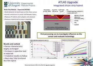
Cu/Ti layer (1 μ m). Passivation (3-4 μ m BCB). 4 μ m Ni + 150 nm Au. Via etched opening in BCB (45 º) coated with Cu/Ti. BCB (6 or 12 μ m) (dielectric). Passivation (SiO 2 ). Al strip. SiO 2. Si bulk. implant. Cross-section of first prototype run:

E N D
Cu/Ti layer (1 μm) Passivation (3-4 μm BCB) 4 μm Ni + 150 nm Au • Via • etched opening in BCB (45 º) • coated with Cu/Ti BCB (6 or 12 μm) (dielectric) Passivation (SiO2) Al strip SiO2 Si bulk implant Cross-section of first prototype run: The first layer of a fully functional hybrid First processing run to investigate influence on the sensor and evaluate technology • Results and outlook • Sensor characteristics largely unchanged • Increase in capacitive load as expected • Irradiation studies to follow • Next step: fully functional thin film hybrid ATLAS UpgradeIntegrated silicon-strip hybrid Research performed in WP4 of the ATLAS UK Upgrade programme Multi-Chip Module – Deposited (MCMD) Build dielectric & metal layers on the silicon sensor Etched connections to sensor and between layers Replaces FE hybrid, pitch-adaptor and substrate Reduces material and increases integration