Download

1 / 14
140 likes | 307 Views
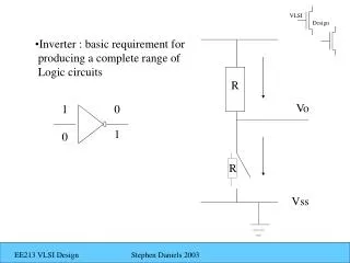
Inverter : basic requirement for producing a complete range of Logic circuits. R. Vo. 1. 0. 1. 0. R. Vss. Vdd. Basic Inverter: Transistor with source connected to ground and a load resistor connected from the drain to the positive Supply rail. Pull-Up. R. Vo.

E N D
Inverter : basic requirement for • producing a complete range of • Logic circuits R Vo 1 0 1 0 R Vss
Vdd Basic Inverter: Transistor with source connected to ground and a load resistor connected from the drain to the positive Supply rail Pull-Up R Vo Output is taken from the drain and control input connected between gate and ground • Resistors are not easily formed in silicon • they occupy too much area Vin Pull Down Transistors can be used as the pull-up device Vss
NMOS Depletion Mode Transistor Pull - Up Vdd • Pull-Up is always on – Vgs = 0; depletion D • Pull-Down turns on when Vin > Vt • With no current drawn from outputs, Ids • for both transistors is equal S Vo V0 Vt Vdd D Vin S Non-zero output Vss Vi
Vin VDD Vo VDD Ids Ids Vgs=0.2VDD Vgs=0 Vgs=-0.2 VDD Vgs=-0.4 VDD Vgs=-0.6VDD VDD –Vds Vds Vgs=VDD Ids Vgs=0.8VDD Vgs=0.6 VDD Vgs=0.4 VDD Vgs=0.2VDD Vds VDD
Vin VDD Vo VDD Decreasing Zpu/Zpd Increasing Zpu/Zpd Vinv • Point where Vo = Vin is called Vinv • Transfer Characteristics and Vinv can be shifted by altering ratio • of pull-up to Pull down impedances
NMOS Depletion Mode Inverter Characteristics • Dissipation is high since rail to rail current flows when Vin = Logical 1 • Switching of Output from 1 to 0 begins when Vin exceeds Vt of pull down device • When switching the output from 1 to 0, the pull up device is non-saturated initially and this presents a lower resistance through which to charge capacitors (Vds < Vgs – Vt)
NMOS Enhancement Mode Transistor Pull - Up Vdd • Dissipation is high since current flows when Vin = 1 • Vout can never reach Vdd (effect of channel) • Vgg can be derived from a switching source (i.e. one phase • of a clock, so that dissipation can be significantly reduced • If Vgg is higher than Vdd, and extra supply rail is required D Vgg S Vo V0 Vdd D Vt (pull up) Vin S Non zero output Vss Vt (pull down) Vin
Cascading NMOS Inverters When cascading logic devices care must be taken to preserve integrity of logic levels i.e. design circuit so that Vin = Vout = Vinv Determine pull – up to pull-down ratio for driven inverter
Assume equal margins around inverter; Vinv = 0.5 Vdd Assume both transistors in saturation, therefore: Ids = K (W/L) (Vgs – Vt)2/2 Depletion mode transistor has gate connected to source, i.e. Vgs = 0 Ids = K (Wpu/Lpu) (-Vtd)2/2 Enhancement mode device Vgs = Vinv, therefore Ids = K (Wpd/Lpd) (Vinv – Vt)2/2 Assume currents are equal through both channels (no current drawn by load) (Wpd/Lpd) (Vinv – Vt)2 = (Wpu/Lpu) (-Vtd)2 Convention Z = L/W Vinv = Vt – Vtd / (Zpu/Zpd)1/2 Substitute in typical values Vt = 0.2 Vdd ; Vtd = -0.6 Vdd ; Vinv = 0.5 Vdd This gives Zpu / Zpd = 4:1 for an nmos inverter directly driven by another inverter
Pull-Up to Pull-Down Ratio for an nMOS inverter driven through 1 or more pass transistors Inverter 1 Inverter 2 Vdd Vdd A B C Vout2 Vin1 It is often the case that two inverters are connected via a series of switches (Pass Transistors) We are concerned that connection of transistors in series will degrade the logic levels into Inverter 2. The driven inverter can be designed to deal with this. (Zpu/Zpd >= 8/1) [ we will demonstrate this later]
Complimentary Transistor Pull – Up (CMOS) Vdd Vtn Vtp Vout P on N off N on P off Vo Vin Both On Vin Vss Vdd Vss Logic 1 Logic 0
Vtn Vtp Vout 1: Logic 0 : p on ; n off 5: Logic 1: p off ; n on 2: Vin > Vtn. Vdsn large – n in saturation Vdsp small – p in resistive Small current from Vdd to Vss 4: same as 2 except reversed p and n 3: Both transistors are in saturation Large instantaneous current flows P on N off N on P off Both On Vin Vss Vdd 1 2 3 5 4
CMOS INVERTER CHARACTERISTICS Current through n-channel pull-down transistor Current through p-channel pull-up transistor If n = pand Vtp = –Vtn At logic threshold, In = Ip Mobilities are unequal : µn = 2.5 µp Z = L/W Zpu/Zpd = 2.5:1 for a symmetrical CMOS inverter
CMOS Inverter Characteristics • No current flow for either logical 1 or logical 0 inputs • Full logical 1 and 0 levels are presented at the output • For devices of similar dimensions the p – channel is slower than the n – channel device