Download
1 / 1
10 likes | 223 Views
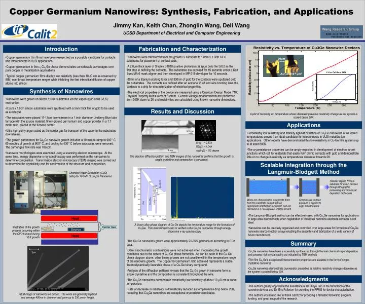
I-V for Cu3Ge at 345K. 5. Current (mA). 0. -5. -10. -0.4. -0.2. 0. 0.2. 0.4. Voltage (V). 30 μ m. A=1.25x10 -9 μ m 2. …Ge. Copper Germanium Nanowires: Synthesis, Fabrication, and Applications Jimmy Kan, Keith Chan, Zhonglin Wang, Deli Wang

E N D
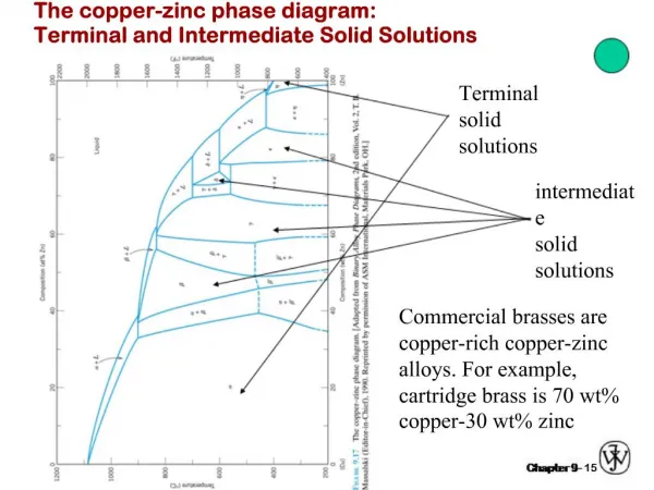
I-V for Cu3Ge at 345K 5 Current (mA) 0 -5 -10 -0.4 -0.2 0 0.2 0.4 Voltage (V) 30μm A=1.25x10⁻⁹μm2 …Ge Copper Germanium Nanowires: Synthesis, Fabrication, and Applications Jimmy Kan, Keith Chan, Zhonglin Wang, Deli Wang UCSD Department of Electrical and Computer Engineering Fabrication and Characterization Introduction • Nanowires were transferred from the growth Si substrate to 1.0cm x 1.0cm SiO2 substrates for placement of contact pads. • A 2.0μm thick layer of Shipley S1818 positive photoresist is spun onto the SiO2 as the first step in defining the contacts. The substrates are exposed for 15 seconds under a Karl Suss MA-6 mask aligner and then developed in MP-319 developer for 10 seconds. • 30nm of a titanium sticking layer and 300nm of gold for the contacts were sputtered onto the substrates. The contacts are defined after an acetone lift off and wire bonding links the contacts to a chip for characterization of electrical properties. • The electrical properties of the device are measured using a Quantum Design Model 7100 Physical Property Measurement System. Current-Voltage measurements are performed from 345K down to 2K and resistivities are calculated using known nanowire dimensions. • Copper germanium thin films have been researched as a possible candidate for contacts and interconnects in VLSI applications. • Copper germanium in the ε1-Cu3Ge phase demonstrates considerable advantages over pure copper in metallization applications. • Typical copper germanium films display low resistivity (less than 10μΩ cm as observed by IBM) over broad temperature ranges while inhibiting the fast interstitial diffusion of copper atoms into silicon. Synthesis of Nanowires • Nanowires were grown on silicon <100> substrates via the vapor-liquid-solid (VLS) mechanism. • 0.5cm x 1.0cm silicon substrates were sputtered with a 5nm thick film of gold to be used as a catalyst. • The substrates were placed 11-13cm downstream in a 1 inch diameter Lindberg Blue tube furnace with the source material, finely ground germanium and copper powder in a 1:1 molar ratio, placed at the furnace center. • Ultra high purity argon acted as the carrier gas for transport of the vapor to the substrates downstream. • The growth parameters for Cu3Ge nanowire growth included a 10 minute ramp to 900° C, 60 minutes of growth at 900° C, and cooling to 400° C before substrates were removed. The carrier gas flow rate was 70sccm. • Nanowire morphologies were examined using a scanning electron microscope. At the same time, energy dispersive x-ray spectroscopy was performed on the nanowires to determine composition. Transmission electron microscopy (TEM) imaging was carried out to determine the crystallinity and for confirmation of the structure and composition. Results and Discussion A plot of resistivity vs. temperature shows decreasing relative resistivity change as the system is cooled below 20K. Applications g2 g1 500 nm • Remarkably low resistivity and stability against oxidation of Cu3Ge nanowires at all tested temperatures proves it an ideal candidate for interconnects in VLSI metallization applications. Other reports have demonstrated this low resistivity in Cu-Ge film systems up to at least 800K. • The cryoresistance properties can be amply exploited in development of electron tunnel junctions which call for materials that easily form ohmic contacts with gold and demonstrate little or no change in resitivity as temperatures decrease towards 0K. D1(g1) ~ 2.87A D2(g2) ~ 4.04A a(g1-g2) ~ 112 degree 4 nm The electron diffraction pattern and TEM images of the nanowires confirms that the growth is single crystalline and composition is consistent. Scalable Integration through the Langmuir-Blodgett Method Chemical Vapor Deposition (CVD) Setup for Growth of Cu3Ge Nanowires Transfer aligned NWs to substrate for use in devices through lithographic processing and monolayer deposition techniques Wires are ultrasonicated to separate them from the substrate, coated with an appropriate amphiphilic surfactant, and are dissolved in a non-aqueous volatile solvent. Compressive surface pressure is applied to align the nanowires. • The Langmuir-Blodgett method can be effectively used with Cu3Ge nanowires for applications in large area interconnects when registration of individual nanowire-electrode contacts is not ideal. • Nanowires can be precisely organized and controlled over large areas for formation of Cu3Ge nanowire interconnection arrays enabling the assembly and fabrication of a wide variety of future nanodevices. A binary alloy phase diagram of Cu-Ge depicts the temperature range for the formation of Cu3Ge. This stoichiometric ratio is verified in the Cu3Ge nanowires through energy dispersive x-ray spectroscopy. Illustration of the growth process occurring within the CVD furnace during VLS growth • The Cu-Ge nanowires grown were approximately 25-35% germanium according to EDX data. • Other stoichiometric combinations were not achieved when modulating the growth conditions due to the nature of Cu-Ge phase formation. As can be seen in the Cu-Ge phase diagram above, other binary phases are not possible within the temperature range of the nanowire growth. The Copper to Germanium ratio achieved represents a stable, thermodynamically favorable phase of a Cu-Ge binary compound. • Analysis of the diffraction patterns reveals that the Cu3Ge grown in nanowire form is single crystalline and the composition is consistent throughout the wire. • The Cu3Ge nanowires demonstrate remarkably low resistivity of about 10 μΩ cm at room temperature. • Rate of decrease in resistivity is dramatically reduced as temperatures drop below 20K, revealing that Cu3Ge nanowires are exceptional cryoresistor candidates. Summary • Cu3Ge nanowires have been successfully synthesized through thermal chemical vapor deposition and possess high crystal quality as indicated by TEM analysis • Thin film Cu3Ge’s exceptional interconnection properties are scalable in the form of single-crystalline nanowires • Cu3Ge nanowires demonstrate cryoresistor properties as relative resistivity changes decrease as the system is cooled below 20K 1μm Acknowledgments • The authors greatly appreciate the assistance of Dr. Xinyu Bao in the fabrication of the nanowire devices and Dr. Eric Fullerton for providing the PPMS for device characterization. • The authors would also like to thank CalIT2 for providing a fantastic fellowship program, funding, and great support of the research. SEM image of nanowires on Silicon. The wires are generally tapered and average 400nm in diameter and grow up to 250 μm in length .