Download
1 / 20
340 likes | 1.52k Views
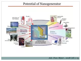
Potential of Nanogenerator. Adv. Func Mater. , 2008 (18) 1-15. Outline. Proof of principle of ZnO nanowires power generation triggered by an AFM tip (Wang et al, Science 2006) Nanoscale generator (Wang et al, Science 2007) and potential applications

E N D
Potential of Nanogenerator Adv. Func Mater., 2008 (18) 1-15.
Outline Proof of principle of ZnOnanowires power generation triggered by an AFM tip (Wang et al, Science 2006) Nanoscale generator (Wang et al, Science 2007) and potential applications Controversy regarding the power generation mechanism
Aligned ZnO NWs grown on Al2O3 • n-type ZnOnanowiregrown on Al2O3 substrate • generating electricity by deforming NW with AFM tip Science, 312 (2006) 242-246.
Output voltage from aligned ZnOnanowires • Sharp output voltage • Peak corresponds to maximum deflection of NW Discharge occurs when tip contacts with compressed side Science, 312 (2006) 242-246.
Mechanism of ZnONanogenerator VL=Vm-VS Transport is governed by metal-semiconductor Schottky barrier for PZ ZnO NW Electron affinity of ZnO: 4.5 eV Work function of Ag: 4.2 eV Work function of Pt: 6.1 eV Science, 312 (2006) 242-246.
The difference of Ohmic and Schottky • No output signal form Al-In-coated Si tip (ohmic contact • with ZnO NW) Adv. Func Mater., 2008 (18) 1-15.
ZnONanogenerator structure Zig-Zag Pt coated Si electrode plays the role of an array of AFM tips Device embedded in a polymer protecting layer Nanogenerator immersed in an ultrasonic bath Schematic view and SEM images of the nanogenerator Direct-Current Nanogenerator Driven by Ultrasonic Waves Wang et al Science 2007, 316 p102
Power generation mechanisms SEM cross-section view of the nanogenerator Equivalent circuit Schematic view of the discharging mechanisms
Power generation Current generated as a function of time Device size: 2mm2 Power generated: 1pW Estimated power per NW: 1-4 fW Power density after optimization (109 active NW per cm2): 1-4 µW/ cm2 Current, bias and resistance of the generator as a function of time
Applications: transistors and LED Current and emission intensity of a carbon nanotubes film as a function of gate voltage (Vd was 1V) Chen J. et al, Science 2005, 310, p1171 a. Gate dependent IV characteristics of a cross NW FET b. SEM image of a cross NW junction, scale bar is 1µm Huang Y. et al, Science 2001 284 p1313 A generator providing 10 to 50nW is required to power such a cross NW FET µW power level needed for a CNT LED
Applications: wireless sensors • Sensor nodes (motes) applications: • Structural monitoring of buildings • Military tracking • Personal tracking and record system (Health) Basic wireless sensor arrangement MEMS accelerometersalreadyused for various applications • Powering motes: • Sensor 12µW quiescent power • ADC 1µW for 8 bit sampling • Transmitter 0.65µW for 1kbps Energy Harvesting From Human and Machine Motion for Wireless Electronic Devices Mitcheson et al, proceedings of the IEEE, Vol 96, N.9, 2008
Piezoelectric transducer for energy harvesting Test: 608 Hz resonantoperation 1g acceleration 0.89V AC peak–peakgenerated 2.16 µW power output Fang HB et al, Microelectronics Journal 37 (2006) 1280–1284 Mitcheson et al, proceedings of the IEEE, Vol 96, N.9, 2008
Electrostatic transducer for energy harvesting Assembled JFET SEM images of the generatorintegratedwith a FET schematicview of a constant charge electrostatictransducer Mitcheson et al, proceedings of the IEEE, Vol 96, N.9, 2008 Generates 100 µW/cm3 from a vibration source of 2.25 m/s2 at 120 Hz S. Roundy, P. K. Wright, and J. M. Rabaey, EnergyScavenging for Wireless Sensor Networks, 1st ed. Boston, MA: Kluwer Academic, 2003. electret: permanent charge buried in the dielectric layer
Argument against Wang Advanced Materials 20, 4021 (2008)
Origin of the piezoelectric voltage • Strain displacive charge • Displacive charge voltage • For ideal insulator: Generation of piezoelectric charge can be considered equivalent to the generation of a potential Gosele et al. Adv. Mater. 20, 4021 (2008)
Model of ZnO Piezoelectric Generator For semiconducting ZnO: Intrinsic time constant τL ~ 10-2ps Load time constant RL = 500MΩ CL > 5pF τL ~ 1s << << Gosele et al. Adv. Mater. 20, 4021 (2008)
Rectification of a Schottky diode V ~ kBT/q ~ 25meV quasi-ohmic To get rectification: V >> Vbi~ 0.3-0.8V Wang’s data: output ~ 10mV Gosele et al. Adv. Mater. 20, 4021 (2008)
Voltage argument Wang et al’s previous opinion: Piezoelectric voltage is 0.3V (calculation)High contact resistance leads to low output of 10 mV (experiment) Gosele et al ruled out the possibility of a high contact resistanceLoad resistor is 500 MΩ no way for a contact resistance higher than 500 MΩ Wang et al. NanoLett. 7, 2499 (2007) Gosele et al. Adv. Mater. 20, 4021 (2008)
Voltageargument Wang et al’s new model:10 mV:difference of Fermi levels0.3V:real Schottky diode driving voltage If Wang’s new model is true,0.3V is still a small voltage to rectify the piezoelectric signal… Wang et al. Adv. Mater. 20, 1 (2008) Wang et al. NanoLett. 8, 328 (2008)
Unknowns behind the nanogenerator ? I. Time constant The nanogenerator model II. Rectification There is a lot of more work to be done…