Download
1 / 16
160 likes | 263 Views
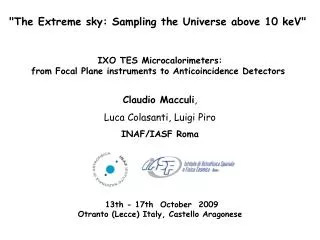
" The Extreme sky: Sampling the Universe above 10 keV". IXO TES Microcalorimeters: from Focal Plane instruments to Anticoincidence Detectors. Claudio Macculi , Luca Colasanti, Luigi Piro INAF/IASF Roma. 13th - 17th October 2009 Otranto (Lecce) Italy, Castello Aragonese.

E N D
"The Extreme sky: Sampling the Universe above 10 keV" IXO TES Microcalorimeters: from Focal Plane instruments to Anticoincidence Detectors Claudio Macculi, Luca Colasanti, Luigi Piro INAF/IASF Roma 13th - 17th October 2009 Otranto (Lecce) Italy, Castello Aragonese
Italian collaboration Piro Luigi Morelli E. (IASF-Bo) Colasanti L. Rubini A. Macculi C. Mastropietro M. (CNR/ISC) Natalucci L. Lotti S. Mineo T. Barbera M. La Rosa Perinati E. Gatti F. Ferrari L. + Tech. personnel Bagliani D. Torrioli G. Bastia P. Bonati A.
Outline • TES microcalorimeter: working Principle • Cryogenics and Readout electronics • Detector Sizes, Single Pixel and Array results • IXO X-ray Microcalorimeter Spectrometer • Cryogenic AntiCoincidence Detector • Preliminary Test • Conclusion • Future: CryoAC as Hard X-ray ray detectors?
The X-ray micro calorimeter consists of a: • X-ray absorber (CABS) • temperature sensor • a thermal link (G) that connects the absorber to a heat bath • A thermal bath to keep the absorber's temperature constant is necessary (restore the Working Point) • Photon absorption Absorber temperature change Change in TES-resistance. Since the TES is Voltage polarised Change in current • Weak currents (also < μA), low TES Resistance (~ 0.1 Ohm) a special low-noise current amplifier is required SQUID Amp. (Superconducting Quantum Interference Device Amplifier) T R I TES microcalorimeter: working Principle …used from Microwave to soft-Gamma ray domain...
Attenuation of thermal bath temperature fluctuations En. Bandwidth En. Resolution Tb/TTES Electro-Thermal Feedback – Energy Bandwidth – Energy Resolution • The Joule heating produced by Voltage bias • PJ = V2/R: • if T R PJ R • Electro-Thermal stability Moreover: strong reduction of the decay time constant fast signals high count rate (bright sources or big area optics) High En. BW High C, Low alfa (wide transition) High En. Res. low T cryogenic detector low C high alfa (narrow transition) Trade off is necessary to reach the wanted performances
3He fridge insert (Kelvinox) Supracon Niobium can for magnetic shielding Magnicon Cryogenics and Readout electronics Cryogenics: 3He/4He mixture (working on phase separation) few-10 mK base temperature (tens to hundred μW@100mK) 4He Pulse tube + ADR (ADR works on paramagnetic salt demagnitazion) about 30 mK base temperature (3 μW@100mK for 20 h operation) Temp. stability: about 10 μKrms (several hours) Readout electronics: SQUID (micro-machined device): Magnetic flux is generated by TES-current flowing in a coil coupled to the SQUID. Such a flux crosses the Josephson junction where it is transformed in Voltage. Noise: few pA/rtHz up to some MHz bandwidth Bias Power: few nW Vericold ADR system Cold finger
EFWHM = 3.6 eV INFN and Genova Univ. Ferrari, Gatti et al. INFN and Genova Univ. Akamatsu, LTD13, in press, (2009) TMU-ISAS Hoevers et al., J Low Temp Phys, 151, (2008) Bandler et al., J Low Temp Phys, 151, (2008) Detector Sizes and Single Pixel results TES on silicon membrane (tech. used for the Array): - Ir/Au, Ti/Au or Mo/Au (total thickness about 1E+2 nm) onto SiN (1 um) suspended membrane (TES area depends on the pxl area) - Absorber (Au, Au/Bi, Cu/Bi, Sn, few um thick) growth on the TES substrate - Pixel about 250x250 um SRON
FDM technique: • Pixels are AC-biased (line by line) • Summing node (column by column) • De-modulation by the same frequency • to recover the pulse 32x32 NASA GSFC – IXO/XMS (bond pads for 256 channels only) Eckart, Doriese, SPIE Newsroom , 2009 What about the Array? • Multiplexing technique is necessary to minimize the heat load caused by thermal conduction through the harness to the cold finger (thousand wires). The array is powered and read by rows or by columns using different Multiplexing methods: • FDM (sinusoidal excitation) • TDM (switch ON/OFF line by line) • CDM (inversion bias polarity)
IXO X-ray Microcalorimeter Spectrometer IXO consortium-CoPI NASA/GSFC, SRON, ISAS-JAXA, INAF/IASF Roma Layout wich fits the IXO Reqs. • Central, core array: • Individual TES • 42 x 42 array with 2.9 arc sec pixels • 2.0 arcmin FOV • 2.5 eV resolution (FWHM) • ~ 300 sec time constant • 0.2-10 keV • Outer, extended array: • 4 absorbers/TES • Extends array to 5 arcmin FOV • 52 X 52 array with 5.8 arcsec pixels • <10 eV resolution • <2 msec time constant Inner Pixel: ~ 300x300 m2 Outer Pixel: ~ 600x600 m2 Absorber: Bismuth 7 m
TES-Array: Cryo-AC Rej eff. = 99% D < 1mm MIP Events to be rejected Cryogenic AntiCoincidence Detector • Bkg requirement: 2·10-2 cts cm2 s-1 keV-1 • Without AC: at least 10 times larger (from preliminary simulation only GCR accounts for 0.15 cts/cm2/s/keV) • Requires an AC with > 95% rejection efficiency • AC need to be < 1mm near to the TES Cryogenic detector
Thickness (μm) Emax (MeV) Saturation Range Primary pr En. (MeV) 100 0.4 0.9-15 150 0.6 1.05-15 CryoAC 200 0.8 1.2-15 18 mm 250 1 1.4-15 300 1.2 1.6-15 Different thickness EMAX and Eth(Epr) if Eth(Epr) > EMAXSaturation 18 mm TES Array 30 mm CryoAC Design We decide for TES-based Cryo AC made of Silicon due to the experience inside our collaboration • Baseline Geometry: Assembly of 4 sub-unit • Detector technology: TES, the same of the focal plane instrument simplification of the Electrical, Mechanical and Thermal I/F ( increase reliability the TRL) • DT Analysis (Cosmic ray flux plus soft protons from mirrors plus Solar flare): • 5% DT To be conservative CryoAC “Total recovery time” < 500 μs • Without Solar Flare, a DT = 1% corresponds to a “Total recovery time” up to 1 ms • “Total recovery time” to be compared with the TES-Array time constant • Expected maximum deposited energy ~ 4 MeV CryoAC Energy Bandwidth: 0.5-1 MeV (to increase BW solving the saturation trade-off with the time constant and Dead Time) • Suppose up to 300 μm thick about 90 keV released from MIP. At least S/N > 10Emin = 5 KeV
Thickness = 300 um 3.3 mm 5 mm Illumination hole SQUID 55Fe Source setup IXO-CryoAC Prototype measurements: Preliminary Test Produced at Genova University ABSORBER Si n-type: 16-27 ohm*cm A ~ 16.5 mm2 TES Iridium V = 3.7mm2 x 90nm EMAX ~ 450 keV
55Fe Source Ib = 650 uA Results: Fast signals and low energy events detected Amplitude Variance under investigation
Conclusion • Results from a detector of C ~ 16.5 pJ/K and A ~ 16.5 mm2 (~ x200 usual pixel area): • Events from 55Fe detected • Fast Rise time ~ 2 μs • Fast Decay time ~ 100 μs for near null ETF we got Fast signals (D TES array ~ 300 μs) • NOT FAR FROM THE GOAL • Next future • Further Investigation for amplitude Variance • Test on 10x10 mm2 pixel, 50 μm thick (V ~ 5 mm3) • Same Volume of the present detector but 6x in Area (final size 18x18 mm2) • It is also foreseen to use 241Am (~ 5.5 MeV) to study the saturation regime (Dead time)
TES 400 μm square W.B. Doriese et al., J Low Temp Phys (2008) 151 Future: CryoAC as Hard X-ray ray detectors? Already exists TES-detector with E/dE > 2000 at 60 keV adopted for nuclear materials analysis Tin bulk absorber (~ 1x1x0.25 mm3) by-layer Mo/Cu TES D.T.Chow et al., Proceedings of SPIE Vol. 4141 (2000) TES: 200 nm thick 57eV@60keV (expected ~ 23 eV)