8251A USART: Programmable Communication Interface Overview
The 8251A is a versatile USART for synchronous/asynchronous serial data communication, featuring programmable peripheral design in a 28-pin DIP package. It receives parallel data from the CPU and transmits serial data, as well as handles external data transfer to the CPU. This encompasses sections like Data Bus Buffer, Read/Write Control Logic, Modem Control, Transmitter, and Receiver, all crucial for efficient data processing and transfer. The chip supports various functions like data transmission, reception, status checking, and error detection, making it an essential component for robust communication systems.

8251A USART: Programmable Communication Interface Overview
E N D
Presentation Transcript
8251A is a USART Universal Synchronous Asynchronous Receiver Transmitter
Used for… • Programmable peripheral designed for synchronous /asynchronous serial data communication, packaged in a 28-pin DIP. • Receives parallel data from the CPU & transmits serial data after conversion. • Also receives serial data from the outside & transmits parallel data to the CPU after conversion.
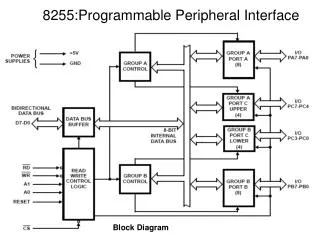
Sections of 8251A • Data Bus buffer • Read/Write Control Logic • Modem Control • Transmitter • Receiver
1. Data Bus Buffer D0-D7 8-bit data bus used to read or write status, command word or data from or to the 8251A
2. Read/Write Control logic • Includes a control logic, six input signals & three buffer registers: Data register, control register & status register. • Control logic : Interfaces the chip with MPU, determines the functions of the chip according to the control word in the control register & monitors the data flow.
Input signals • CS – Chip Select : When signal goes low, the 8251A is selected by the MPU for communication. • C/D – Control/Data : When signal is high, the control or status register is addressed; when it is low, data buffer is addressed. (Control register & status register are differentiated by WR and RD signals) • WR : When signal is low, the MPU either writes in the control register or sends output to the data buffer. • RD : When signal goes low, the MPU either reads a status from the status register or accepts data from data buffer. • RESET : A high on this signal reset 8252A & forces it into the idle mode. • CLK : Clock input, usually connected to the system clock for communication with the microprocessor.
Control Register • 16-bit register for a control word consist of two independent bytes namely mode word & command word. • Mode word : Specifies the general characteristics of operation such as baud, parity, number of bits etc. • Command word : Enables the data transmission and reception. • Register can be accessed as an output port when the Control/Data pin is high.
Status register • Checks the ready status of the peripheral. • Status word in the status register provides the information concerning register status and transmission errors. Data register • Used as an input and output port when the C/D is low
3. Modem Control • DSR - Data Set Ready : Checks if the Data Set is ready when communicating with a modem. • DTR - Data Terminal Ready : Indicates that the device is ready to accept data when the 8251 is communicating with a modem. • CTS - Clear to Send : If its low, the 8251A is enabled to transmit the serial data provided the enable bit in the command byte is set to ‘1’. • RTS - Request to Send Data : Low signal indicates the modem that the receiver is ready to receive a data byte from the modem.
Output Register Transmitter Buffer Transmit control 4. Transmitter section • Accepts parallel data from MPU & converts them into serial data. • Has two registers: • Buffer register : To hold eight bits • Output register : To convert eight bits into a stream of serial bits.
The MPU writes a byte in the buffer register. • Whenever the output register is empty; the contents of buffer register are transferred to output register. • Transmitter section consists of three output & one input signals • TxD - Transmitted Data Output : Output signal to transmit the data to peripherals • TxC - Transmitter Clock Input : Input signal, controls the rate of transmission. • TxRDY - Transmitter Ready : Output signal, indicates the buffer register is empty and the USART is ready to accept the next data byte. • TxE - Transmitter Empty : Output signal to indicate the output register is empty and the USART is ready to accept the next data byte.
Input Register Receive Buffer Receive control 5. Receiver Section • Accepts serial data on the RxD pin and converts them to parallel data. • Has two registers : • Receiver input register • Buffer register RxD RxRDY RxC
When RxD goes low, the control logic assumes it is a start bit, waits for half bit time, and samples the line again. If the line is still low, the input register accepts the following data, and loads it into buffer register at the rate determined by the receiver clock. • RxRDY - Receiver Ready Output: Output signal, goes high when the USART has a character in the buffer register & is ready to transfer it to the MPU. • RxD - Receive Data Input : Bits are received serially on this line & converted into a parallel byte in the receiver input register. • RxC - Receiver Clock Input : Clock signal that controls the rate at which bits are received by the USART.