Download
1 / 58
660 likes | 969 Views
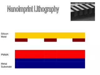
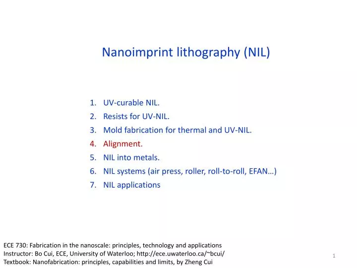
Nanoimprint lithography (NIL). UV-curable NIL. Resists for UV-NIL. Mold fabrication for thermal and UV-NIL. Alignment. NIL into metals. NIL systems (air press, roller, roll-to-roll, EFAN…) NIL applications. ECE 730: Fabrication in the nanoscale : principles, technology and applications

E N D
Nanoimprint lithography (NIL) UV-curable NIL. Resists for UV-NIL. Mold fabrication for thermal and UV-NIL. Alignment. NIL into metals. NIL systems (air press, roller, roll-to-roll, EFAN…) NIL applications ECE 730: Fabrication in the nanoscale: principles, technology and applications Instructor: Bo Cui, ECE, University of Waterloo; http://ece.uwaterloo.ca/~bcui/ Textbook: Nanofabrication: principles, capabilities and limits, by Zheng Cui
Alignment (overlay) • Electronic devices such as transistors/chips require multiple levels of materials and processing. • For NIL, there is no distortion due to lens since no lens is used. • Challenges for sub-100nm alignment: • Smaller error budget for mold pattern placement since it is 1. • Alignment mark fabrication error has to be <10nm. • Features are too small to be seen optically 10nm. • Alignment is sensitive to the gap between mold and substrate. • Mold distortion/drift due to pressure, temperature and defects is big problem. • Generally, alignment for NIL is much more difficult than other lithographies. • Thermal NIL is worse due to thermal expansion mismatch.
Possible alignment methods • Direct imaging, as in optical lithography. • Amplitude-sensitive schemes. • Phase-sensitive schemes. • Spatial phase detecting – Moiré pattern (simple, insensitive to gap) (Wikipedia) In physics, a moiré pattern is an interference pattern created, for example, when two grids are overlaid at an angle, or when they have slightly different mesh sizes. A moiré pattern, formed by two sets of parallel lines, one set inclined at an angle of 5° to the other.
Direct imaging • Backside alignment because silicon substrates are not transparent to visible light. • Sub-micron precision is demonstrated. • Precision is limited by optical resolution and thermal, mechanical noises. • For thermal (or UV) NIL that requires high pressure, alignment is easily destroyed due to lateral drift of mold or substrate.
Amplitude sensitive alignment scheme Maximum signal when aligned. Minimum signal when aligned (I1=I2) William Moreno, Princeton
Two step alignment using cross marks and Moiré patterns • Moiré patterns: optical image of superposition of two patterns. • Advantage: slight displacement of one of the objects creates a magnified change in their Moiré patterns. • For sub-100nm alignment: • Coarse alignment using cross marks and boxes or circular gratings. • Fine alignment using interferometric spatial phase matching (Moiré). • Same as alignment in contact/proximity optical lithography. • Cross mark provide alignment of 0.5μm. • Cross marks are relatively big and easy to locate. Coarse alignment marks
Circular gratings Misaligned Aligned Circular patterns produce more precision for the coarse alignment in the x and y axis. They are more sensitive to displacement than cross marks. M. King and D. Berry were the first who start alignment using moiré concentric circles in 1972 ( Appl. Opt.11. 2455).
Fine alignment using Moiré: concept and simulation Sub-10 nm alignment accuracy Interference Pattern P3 P1 P2 P2 To frame grabber And computer P1 CCD P2 P1 P1 P2 Substrate Stamp Partially reflecting mirror Light source Aligned Out of align Imaging Lens Mask P1 P2 Simulations of alignment/misalignment Substrate P3 = (P1 x P2) / |P1 – P2|
Interferometric spatial phase matching of linear gratings • Challenges: • Precise alignment in tilting. • Grating fabrication error need to be very small, smaller than 10nm. E. Moon, J. Vac. Sci. Tech. 1993A. MoelJ. Vac. Sci. Tech. 1995
Result of sub-100nm alignment in NIL For UV-NIL, sub-100nm alignment can be achieved readily, but this is still too far away from requirement for IC production (few nm). “Sub-20-nm Alignment in Nanoimprint Lithography Using Moiré Fringe”, Li, Nano Lett., 2006.
Nanoimprint lithography (NIL) UV-curable NIL. Resists for UV-NIL. Mold fabrication for thermal and UV-NIL. Alignment. NIL into metals. NIL systems (air press, roller, roll-to-roll, EFAN…)
NIL directly into metals Silicon mold (inset: cross-section) produced by ICP-DRIE (26 cycles), with line-width 1 or 2μm (depth 6μm) and holes with edge length 4μm (depth 8μm). Microstructured silver plate after forming at 400°C with a pressure of 300MPa, and Si mold removal by KOH etching. (Typical thermal NIL pressure is 2MPa) “Metal direct nanoimprinting for photonics”, Buzzi, MEE 2008
NIL directly into metals: bi-layer and sharp mold Fig. 1. Schematic diagrams of imprint technologies. Conventional nanoimprint lithography. Direct imprint metal films. Nanoimprint in metal/polymer bi-layer. “Directly patterning metal films by nanoimprint lithography with low-temperature and low-pressure”, Chen, MEE 2006
Results Fig. 5. The depth of surface-profile in metal films can be tuned by using different imprint pressure (a) 7 MPa, (b) 12 MPa, (c) 14 MPa, (d) 17 MPa. Fig. 2. SEM images of molds (a) conventional binary mold with flat top, (b) sharp mold, (c) triangle mold.
NIL into metal nano-particles at low temperature & pressure Thermal (melting) characteristics of SAM-protected Au nano-particles (NPs). NP can be melted/imprinted at rather low temperature. (SAM: self assembled monolayer) Melting temperature of Au NPs with different sizes. Resistivity (dotted line represents bulk gold resistivity 2.65μΩ·cm). Melt to form continuous film with low resistivity. Reflectivity at 514.5nm wavelength. Insets represent the optical images of NP film before (left) and after (right) the melting. Mass change at various heating temperatures. TEM Melting temperature (K) Resistivity (Ohm cm) Particle diameter Temperature (oC) Weight loss (%) Reflectivity Temperature (oC) Temperature (oC) “Direct Nanoimprinting of Metal Nanoparticles for Nanoscale Electronics Fabrication”, Ko, Nano Lett. 2007
NIL into Au nano-particles and melting of NPs (A, B) Dispensing NP solution on Si wafer. (C, D) Pressing PDMS mold on NP solution under 5psi pressure at 80°C (1atm=14psi). (E, F) Removal of mold and induce NP melting on hot plate at 140°C. The SAM-protected NPs are suspended in an organic solvent that is extremely viscous (like a solid) at room temperature, but its viscosity drops drastically with temperature.
Results of NIL into Au Optical dark field images of (A) nanodots and (C) nanowires (scale bar is 5 μm). AFM topography images of (B) nanodots; (D(i−iv)) straight nanowires, and (D(v)) serpentine nanowires.
c d e mold substrate a molten layer b Laser-assisted direct imprint (LADI) of metals Metal can be easily melted and patterned by a pulsed laser. One-step patterning process: Replaces the steps of resist patterning, pattern transfer by etching, and resist removal all into one single step. And this step takes only order 100 ns! Minimal heating of the substrate Mold and substrate can have different thermal expansion. Application: IC interconnect, flexible/durable NIL metal mold.
200 nm period grating patterned by LADI Cu, 0.24J/cm2 Al, 0.22J/cm2 Pattern height: 100 nm. XeCl excimer laser, =308nm, 20ns pulse, laser fluence 0.24J/cm2 = 12MW/cm2 Line was rounded due to surface tension and volume shrinkage upon solidification.
Ni quartz Ni quartz 200 nm period grating patterned by LADI: Ni Front side illumination, 0.41 J/cm2 Back side illumination, 0.60 J/cm2
F=2R F=L L r W How much pressure needed • Pressure surface tension / dimension. • Order 102atm is needed for 100 nm feature size, due to the high surface tension of metals. • The surface tension of metals are order 1N/m, as compared to 0.07N/m for water.
L L L y Quartz mold h0 x h0 Liquid metal Solid metal Substrate How big feature can be patterned (how far the liquid can flow before it freezes) Inertial force is ignored. p: pressure. : melting time. : viscosity. Experiment: 17 m Si has been patterned, but failed for several tens of m. Viscosity for molten metals are comparable to that of water at room temperature (0.00091 Pasec, or 0.91 centipoises), much lower than polymer.
Direct imprint into Si Faithful duplication of sub-10nm features in the quartz mold due to RIE trenching effect. The reflectivity of a HeNe laser beam from the silicon surface versus the time, when the silicon surface is irradiated by a single laser pulse with 1.6mJ/cm2fluence and 20ns pulse duration. Molten Si, becoming a metal, gives a higher reflectivity. The measured reflectivity shows the silicon in liquid state for about 220ns. Chou, “Ultra fast and direct imprint of nanostructures in silicon”, Nature, 2002
Ultrafast (order 100ns) thermal NIL into polymer resist (not metal) using laser pulse LAN: laser assisted nanoimprint lithography. Polymer resist need to be dye-doped for optical energy absorption (transparent otherwise). Scanning electron microscope (SEM) image of 200 nmperiod grating quartz mold. NPR-69 (a NIL resist) gratings ona Si substrate produced by LAN with a single laserpulse of 0.4J/cm2. The gratings have a line-width of 100nm and height 90nm. Here the UV light is just to melt the resist, rather than curing it. “Ultrafastpatterning of nanostructures in polymers using laser assisted nanoimprint lithography”, Xia, APL, 2003
Nanoimprint lithography (NIL) UV-curable NIL. Resists for UV-NIL. Mold fabrication for thermal and UV-NIL. Alignment. NIL into metals. NIL systems (air press, roller, roll-to-roll, EFAN…)
Limitations of solid parallel plate (SPP) press Ideal SPP Imperfect plate surfaces Uneven mold/substrate backside Non-parallelism between plates Curved sample surfaces Fortunately, most of the problems can be solved by putting a piece of clean room paper, plastics, or graphite sheet above/below mold/substrate.
Air cushion press (ACP) nanoimprint Mold/substrate sealed between plastic sheets/membranes 8-in pressure indicating papers (gas pressure= 5kg/cm2). Uniform color means uniform pressure. A 12-inch imprinted wafer One can get similar imprint result using solid plate press, but needs higher pressure to make sure the pressure is high enough everywhere across the wafer. J. Vac. Sci. Technol. A, Vol. 23, No. 6, pp. 1687-1690, Nov. 2005.
NIL tools: air-press Air press has uniform pressure, but for most applications parallel plate press can also achieve good result (may need something soft like a paper for more uniform pressure). “Air Cushion Press for Excellent Uniformity, High Yield, and Fast Nanoimprint Across a 100 mm Field”, Nano Lett. 2006.
NIL onto curved surface • Imprinted patterns on 2-inch convex surface. • Using flexible PDMS mold and uniform gas pressure, the patterns can be transferred onto curved surface successfully.
Curved surface imprint SEM images of detailed imprinted patterns on curved substrate. J. Vac. Sci. Technol. B, Vol. 24, No. 4, Jul/Aug, pp. 1724-1727, Nov. 2006.
Roller NIL Imprints using a cylinder mold. Imprints using a flat mold: putting the mold directly on the substrate, and rotating the roller on top of the mold. • For schema (a), infinitely large surface area can be imprinted using one (small) mold. • For schema (b), NIL can be done at very low force.
Results of roller NIL AFM graph of a compact disk mold before bent into a cylinder: 700nm tracks pattern on the surface of compact disk. PMMA imprinted by a cylinder mold, showing sub-100nm accuracy in pattern transfer. “Roller nanoimprint lithography”, Tan, JVST B, 1998.
Roll-to-roll (R2R) nanoimprint lithography Mold Schematic of the R2R-NIL process, and the continuous fabrication of a metal wire-grid polarizer as one of its applications. The coating unit. The Imprint unit of the R2R-NIL apparatus. Application: large area electronics (display…) or optical devices (with nano-features) on flexible plastic substrates. “High-Speed Roll-to-Roll Nanoimprint Lithography on Flexible Plastic Substrates”, Guo, Adv. Mater. 2008.
Results of roll-to-roll imprint a) The original Si mold. b-c) Epoxy-silicone gratings replicated from the ETFE mold. d,e) SEM pictures of 200nm period 70nm line- width epoxy-silicone pattern. f) 100nm period 70nm line-width epoxy-silicone pattern
Results of roll-to-roll imprint • Thermal R2R-NIL results: a-b) photograph and SEM of a 700nm period 300nm line-width PDMS grating pattern imprinted on PET strip. • UV R2R-NIL results: c-e) photographs and SEM of 700nm period 300nm line-width epoxy-silicone grating pattern imprinted on PET strip, showing bright light diffraction. Total length is 570mm.
Electric field assisted NIL (EFAN) Principle of EFAN: a voltage is applied between the conductive layers on the mold and the substrate, generating an electrostatic force to press the mold into the resist layer.
EFAN process flow Calculated effective electrostatic pressure (P) versus the required strength of the electric field.
A more accurate calculation A 2D simulation of EFAN, which adds complete details of dielectric structures into the calculation of electric field.
Nanoimprint lithography (NIL) UV-curable NIL. Resists for UV-NIL. Mold fabrication for thermal and UV-NIL. Alignment. NIL into metals. NIL systems (air press, roller, roll-to-roll, EFAN…) NIL applications
NIL applications: overview • Basically, NIL can be used for virtually any applications involving nanofabrication. • In fact, it would be the only choice for high volume production of nano-devices except those in IC (integrated circuit) industry and those don’t need precise patterning (i.e. no need of long range ordering, they can then be patterned by cheap chemical synthesis or self assembly, namely “bottom –up” methods). • This is simply because other nano-lithographies (EBL, FIB, scanning probe…) don’t have the throughput needed for mass production. • The major challenges for NIL: mold fabrication (1), alignment, defect control. It still has a long way to go for IC manufacturing. This section will not be covered in the final exam, but I hope you find it interesting.
HD-DVD Compact disk Magnetic disk Polymer reactor DNA electrophoresis chips Data storage Bio-medical Nanoimprint lithography Others Opto- electronics Display Nano- electronics Nano integrated probe array SAW MLCC Lotus effect product Gecko tape Active field emitting cooling device Photonic crystal Waveguide WDM Grating QD OE HOE Liquid crystal alignment Polarizer Diffuser Diffractive grating FED SET Nano resist pattern Molecular electronics Single electron devices NIL applications
First single-electron memory with 8nm dot using NIL For single electron devices, the size of the quantum dot is very critical. It is achieved by e-beam lithography and size shrinkage techniques, which has very low yield. By using NIL, once the “right” size is achieved, it can be duplicated many times faithfully.
Nano-contact for molecular electronics Austin and Chou, “Fabrication of nanocontacts for molecular devices using nanoimprint lithography”, J. Vac. Sci. Technol. B, 20, 665-667 (2002)
Sub-wavelength optical elements – optical chips by NIL Zone plate of 70 nm min. feature
Thin film reflective polarizer Resist: 15k PMMA 200nm-thick Temperature: 175C Metal grating 5nm-Cr/70nm-Au Grating pitch:190nm Line-width: 70nm Depth: 200nm Yu and Chou, “Reflective polarizer based on a stacked double-layer subwavelength metal grating structure fabricated using nanoimprint lithography”, Appl. Phys. Lett. 77, 927-929 (2000).
Micro-ring resonator Resonant condition: optical path of the ring = n Chao and Guo, “Polymer microring resonators fabricated by nanoimprint technique” J. Vac. Sci. Technol. B, 20, 2862-2866 (2002)
Commercial CD CD is made by hot-embossing into polycarbonate using a Ni mold, very similar to NIL. Compact Disc 650 MB, 48 Mbit/cm2
Nano-CD CD areal density: 400 Gbit/in2 Krauss and Chou, “Nano-compact disks with 400 Gbit/in2 storage density fabricated using nanoimprint lithography and read with proximal probe”, Appl. Phys. Lett. 71, 3174-3176 (1997).