Download

1 / 31
310 likes | 328 Views
This document outlines the specifications and testing results of the front-end DAQ system components for the Belle-II CDC, including ASIC details, signal processing, beam testing, temperature compensation, and grounding considerations. The report highlights test results, ongoing challenges, and future plans for system improvement.

E N D
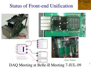
Status of the CDC front-end/DAQ Shoji Uno (KEK) 2012.1.16 Trigger and DAQ workshop
ASIC Level shift to match FADC input Amp-Shaper-Discriminator (ASD) chip ×10 DOUT Single end Specifications TCSP 64pin package 8mm × 8mm 10th B2GM 2
ASIC: Waveform Input : 0.13pC ~ 8 ns The peaking time is defined by transition time from 10% to 90% of the height. Analog output 1MΩ AC couple with probe. Digital output 50Ω DC couple with LEMO cable This digital signal is displayed too low height because it is terminated with 50Ω 10th B2GM 3
ASIC: Gain Output is linear up to 400mV at 0.4pC. Maximum output is 900mV at 8pC. Measurement : 1.06V/pC Design: 1.1V/pC Inputcharge(pC) Measured values are consistent with design values. 10th B2GM 4
ASIC: Gain for digital part Offset Threshold (V) Setting Offset – Setting Input charge (pC) Gain:7V/pC ( design:15V/pC) Output saturate at 0.3pC input.
Gain variation Vth at 10fC input(V) Gain (V/pC)
Readout board Version 0 in 2009 Version 1 in 2010 Version 2&3 in 2011 New ASIC Smaller weight 400g 240g Smaller size 190mmx150mm
Block diagram ASD (ASIC) Gain =1.1V/pc (Analog) + =7V/pc (Digital) Vth DAC Network Proc. Ring Buf. (5msec) + Multi-Trigger Buf. (15) + Data Gen. (FPGA) Detector Sigs. ADC 10bit 30Msps (AD9212) Shaped sigs. PC 48 TDC 1nsec (FPGA) Trigger Discriminated sigs. To trigger logic 8
Signal Shape Raw data mode
Data 2mV/count in FADC Suppress mode
Beam test results Beam incident angle [deg.] Beam incident angle [deg.]
Two modes in data transfer Setting parameter or • Raw data mode • Whole FADC data and TDC data within time window • Low rate, Pedestaldata • Suppress data mode • Two fastest TDC data and sum of FADC data within time window • Multi-trigger • High rate • Pedestal data should be transferred before data taking
Data Time window (~600nsec) Vth for digital signal in ASIC Threshold for sum of FADC data in firmware FADC value - Pedestal TDC1 TDC2 TDC data Channel Sum of FADC data
Dead Time Suppress Mode Linear part is independent on performance of readout PC 0.5%/10kHz Recently, T. Uchida found a bug in the firmware. It will be reduced by factor ~10.
Belle2Link Test • Many efforts were done by IHEP people, KEK DAQ group, T. Uchida, and N. Taniguchi. • Especially, slow control. • Finally, CDC data can be read out using Belle2Link. • Detail will be reported by DAQ people. • Obviously, more tests are necessary.
Trigger I/F • A simple test of TRG I/F wasdone at the beam test. • Detail will be reported by TRG people. • Again, more tests are necessary.
Problem and future plan • Confirm the TRG I/F and Belle2Link • On going. • Study a dead time • 0.5% @10kHz, measured value at the beam test • Fixed. • Estimate FPGA resource at the final version. • Current version is 40% (including TRG I/F and SiTCP) • Data error occur by variations of power supply voltages. • More tests are necessary. • Baseline voltage variation by temperature • Fixed. • Modification will be done in this week.
Temperature dependence of Baseline voltage After compensation Present: Resistor only Baseline Voltage (V) One thermistor Two thermistors All Temperature (℃)
Radiation Test for ASIC • Amount of irradiation • No serious deterioration, so far.
Grounding CDC ground was separated from Belle structure, BPID and SVD. Signal ground was connected on the ground through the shaper board in the electronics hut and also was connected the backward endplate in the CDC. High voltage ground was connected on the ground through the high voltage module in the electronics hut and also was connected the forward endplate in the CDC. There are no serious ground loop problems.
Belle-II CDC grounding CDC ground should be separated from Belle-II structure, BPID, SVD and other sub-detectors. We want to connect the signal ground to the backward endplate in the CDC and also that should be connected to the ground through the power modules in the electronics hut. High voltage ground can be disconnected from the forward endplate, if necessary.
CDC cabling Power cables HV cables Option Low voltage distribution modules
Belle2Link implementation From T. Uchida • An FPGA code of the frontend electronics will not be fixed until the experiment started. • A sanity check of the electronics should be done by a detector group. It is better to implement the link by each detector group.
Requests to the DAQ team From T. Uchida • Providing an FPGA library of Belle2Link and their documents, • We can implement the link individually. • Providing a test bench for the Belle2Link at KEK. • We can debug the link implementation and check normality. To implement the link by each detector group,
Summary • New ASIC works fine. • Mass production is going on. • New 48ch board (Version 3) basically works fine. • More tests for TRG I/F and Belle2Link are necessary. • Data error occurs in variation of power supply voltages. • Should be avoided. • Position and direction of connector will be modified. • We have more space, now. • All problems should be fixed and modification should be done in 2012. Then, board mass production will be done in 2013 (and 2014).
Belle-II CDC Readout Module PCB of 12 layers For the detector • Thickness =1.476mm Test pulse input ASICs ADCs FPGA Trigger Input TRG I/F 150mm DAQ I/F 190mm Power ±5V, +3.3V, +1.8V, +1.0V 28 10th B2GM
Just one track A signal of the gas chamber varies even for one track. Duration is also quite long (~300nsec).