Download
1 / 15
150 likes | 299 Views
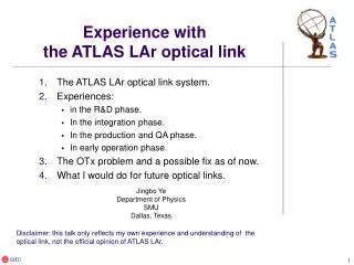
Status report on the LAr optical link. Introduction and a short review. The ASIC development. Optical interface. Conclusions and thoughts. Jingbo Ye SMU. Introduction and a short review. Optical link for 100 Gbps per front-end board:. Front-end. Back-end. clk. data. 10G fiber.

E N D
Status report on the LAr optical link Introduction and a short review. The ASIC development. Optical interface. Conclusions and thoughts Jingbo Ye SMU
Introduction and a short review • Optical link for 100 Gbps per front-end board: Front-end Back-end clk data 10G fiber Interface to ADC, data formatting and encoding. ORx (COTS) 10G copper clk data SerDes embedded FPGA Serializers (LOCsx) clk data 10G copper OTx (LDD + VCSELs) Front-end components are ASICs and custom assembly. VCSEL, fiber, ORx identification, and the back-end development benefit from the Versatile Link common project. ASICs are based on 0.25 µm SOS CMOS. 10G fiber Lar Week Munich April 2011
Introduction and a short review • ASIC prototype at 5 Gbps – LOCs1: • Ring oscillator based PLL provides clocks around 2.5 GHz • 16:1 CMOS multiplexer has a tree architecture • 5 Gbps serial data output through a differential CML driver • Submitted for fabrication in Aug 2009 and delivered in Nov 2009 Lar Week Munich April 2011
Introduction and a short review • ASIC prototype at 5 Gbps – LOCs1: 5 Gbps Lar Week Munich April 2011
Introduction and a short review • ASIC prototype at 5 GHz – LCPLL: • Measurement results: • Tuning range: 4.7 to 5 GHz. Simulation: 3.79 to 5.01 GHz. • Power consumption: 121 mW at 4.9 GHz. Compare: ring oscillator based PLL, 173 mW at 2.5 GHz • Random jitter: 1 - 2.5 ps (RMS) • Deterministic jitter: < 17 ps (pk-pk) Lar Week Munich April 2011
ASIC development • Steps from LOCs1 of 5 Gbps to LOCsx, the 10 Gbps version: • Initially thought that we would move from LOCs1 to LOCs6. • Difficulties were found in the 5 GHz clock fan-out over the whole chip of the size of about 2 mm × 6 mm. This is limited by the GC process (0.5 µm trace) we have evaluated to be rad-tol, and are used in the LOCs1 development. • A faster PC process (still 0.25 µm, but also 0.25 µm trace) will come out April 2011, and 0.18 µm later part of 2011. Either may get us back to the LOCs6 concept if we so choose at that time. • We now propose to step back to LOCs2: two serializing units with one LC PLL clock in a chip. • We will then need to move the switch for the redundancy channel into the interface chip, in front of the LOCs2 chip. Data 16:1 Serializer 10 Gbps Clock 5 GHz LC PLL Data 16:1 Serializer 10 Gbps LOCs2 Lar Week Munich April 2011
ASIC development • We are working on the fast (CML) parts in this design. They are the shapes in orange: the clock buffer, the LC VCO, the first stage Div2, the last stage 2:1 MUX, and the CML driver. • We also realized that with the GC process, we may only push up to 8 Gbps (ss corner, 85C). We will rely on the new PC process and the 180 nm feature size to get us to 10 Gbps. • New irradiation tests will be needed on the new processes. Lar Week Munich, April 2010
ASIC development • The clock buffer: common centroid layout. Lar Week Munich April 2011
ASIC development • GC process v.s. PC (true 0.25 µm), preliminary. • Metal trace: 0.9 µm 0.4 µm • space between trace: 0.8 µm 0.4 µm • Via: 0.6 µm 0.4 µm • Contact: 0.6 µm 0.4 µm. • PC process reduce the layout area by ~40% (ex. clock buffer) • PC process Improve 10-15% in CML buffer but only 3% in a CMOS inverter. PC: 27.5 × 48.3 µm2 GC: 38.8 × 57.4 µm2 Lar Week Munich April 2011
ASIC development • The CML divider (by 2): Lar Week Munich April 2011
ASIC development • The CML output driver: • At TT corner and 8 Gbps, DJ < 20 ps 27 C 55 C 85 C Lar Week Munich April 2011
ASIC developments Eye at 8 Gbps 27 C 55 C 85 C SS FF Lar Week Munich April 2011
ASIC next steps • We are still working on the CML 2:1 multiplexer. • We need to fine tune the LC VCO. • After that an overall and optimized CML circuits layout will be carried out. • Follow that will be the CMOS circuits part and overall timing adjustment. • So far all the design is based on the GC process. We will need to decide on whether we prototype the GC design, or move to the PC design. Lar Week Munich April 2011
Optical interface and the back-end • The form factor of this optical interface is not decided. • Many factors need to be considered: • System reliability. Possible failure modes. • Real state on the FEB front panel. • Ease of installation. • Experience in the Versatile Link project is very valuable. • The development of OTx (LDD identification or ASIC design, mechanical packaging) has started (BNL, SMU). Support has been requested in the new DOE generic detector development program. • The VCSEL and fiber have been identified in the Versatile Link project. • The link back-end has been developed in the Versatile Link project, or at least a similar design can be adapted. Lar Week Munich April 2011
Conclusions and thoughts • The LOC ASIC development is progressing as planned. A lot of details are not reported here. We would like to call for a review after we have the post layout simulation results on all the CML circuits. • We benefit from developments in the Versatile Link project in the optical link system spec development, the optical interface (the optical transmitter and receiver, the fiber and connector) development, as well as the back-end FPGA evaluation,. • We would like to start system level discussions with the link’s up- and down-stream electronics, or on a higher level, the discussion about the design and demo of the FEB2 and the ROD2. Lar Week Munich April 2011