Download
1 / 25
290 likes | 539 Views
Modern Laser Technologies for Fabrication of Solar Cells. V.E. Kisel , A.E. Gulevich and N.V. Kuleshov Belarusian National Technical University, Center for optical materials and technologies, Nezavisimosti Avenue, 220013 Minsk, Belarus,

E N D
Modern Laser Technologies for Fabrication of Solar Cells V.E. Kisel,A.E. Gulevich and N.V. Kuleshov Belarusian National Technical University, Center for optical materials and technologies, Nezavisimosti Avenue, 220013 Minsk, Belarus, phone/fax :+375 17 292 62 86, e-mail: nkuleshov@bntu.by UN/Belarus Workshop, Minsk, 2013
Outline 1. Introduction: CIGS solar cells 2. Yb:KYW femtosecond laser for scribing 3. Experimental results 4. Yb:KYW regenerative amplifier 5. Summary and Outlook UN/Belarus Workshop, Minsk 2013
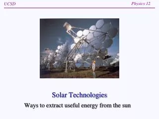
Photovoltaic (PV) production World Solar Power Topped 100,000 Megawatts in 2012 Solar panels on the Int Space Station Camel with solar panel for refrigerator UN/Belarus Workshop, Minsk 2013
Mainstream thin film PV technologies • silicon (Si) • cadmium telluride (CdTe) • copper indium gallium selenide(CuIn1-xGaxSe2 or CIGS) Advantages of CIGS among other PV • strong absorption of sunlight (1-2 mm layer thickness) • CIGS can be deposited on flexible substrates • polycrystalline form of deposition • highest efficiency (around 20%) among thin-film solar cells UN/Belarus Workshop, Minsk 2013
CIGS-based thin-film solar cell structure Top contact ZnO:Al 0.5 μm ZnO window 30 nm CdS buffer layer 1,5 μm CuInxGa1-xSe2(CIGS) absorber (active layer) 0.7-1 μm back contact (molybdenum) Glass substrate [1] A. E. Delahoy, L. Chen “Advanced CIGS Photovoltaic Technology”, Annual Technical Report–Phase II 15 November 2002–14 November 2003, NREL/SR-520-35922, May 2004 UN/Belarus Workshop, Minsk 2013
Scheme of the CIGS-based thin-film solar cell battery ZnO:Al ZnO:Al ZnO:Al ZnO ZnO ZnO CdS CdS CdS CIGS CIGS CIGS Mo Mo Mo Glass Substrate 1st scribing process (P1): Molybdenum (Mo) contact (leave the Glass undamaged) 2nd scribing process (P2): CdS+CIGS (leave the Mo undamaged) 3rd scribing process (P3): ZnO:Al+ZnO+CdS+CIGS (leave the Mo undamaged) UN/Belarus Workshop, Minsk 2013
Molybdenum thin-film Molybdenum SUBSTRATE Thickness: 700 nm Melting temperature: 2600 ºC Evaporation temperature : 6800 ºC UN/Belarus Workshop, Minsk 2013
Nanosecond pulse laser scribing Drawbacks • Melting zone • Micro cracks • Blast wave 4. Heating zone 5. Temperature transmission 6. Splinters [2]A.D. Compaan, I. Matulionis, S. Nakade “Laser scribing of polycrystalline thin films”, OLE 34 (2000) 15-45 UN/Belarus Workshop, Minsk 2013
Ultrashort pulse laser micromachining Direct evaporation of metal • No melting • No micro cracks • No blast wave 4. No heating zone 5. No temperature transmission 6. No splinters [3]C. Momma, S. Nolte, B.N. Chichkov, F.v. Alvensleben, A.Tunnerbaum, “Precise laser ablation with ultrashort pulses”, Appl. Surf. Sci. 109/110, 15-19 (1997) UN/Belarus Workshop, Minsk 2013
Scheme of directly-diode-pumped Yb:KY(WO4)2 femtosecond laser UN/Belarus Workshop, Minsk 2013
Yb3+:KY(WO4)2 Laser Crystal • strong absorption band near 980 nm • direct diode-pumping • low quantum defect • low heat generation • broad gain bandwidth(20-30 nm) • femtosecond pulse generation 50 mm Crystal growth at Plant “Optik”, Lida, Belarus UN/Belarus Workshop, Minsk 2013
Dielectric mirror Bragg reflector GaAs Substrate InGaAs Quantum Well Structure Schematic of SESAM Laser light Developed in cooperation with the Institute of Semiconductor Physics, Novosibirsk, Siberian Branch of RAS UN/Belarus Workshop, Minsk 2013
Pilot femtosecond Yb:KYW laser 1. Output power: 1.5W 2. Pulse duration: 150fs 3. Pulse rep rate: 70MHz 4. Pulse energy: 21.5 nJ 5. Wavelength: 1040 nm 6. TEM00 M2<1.2 7. Pump power6 W In cooperation with SOLAR LS, Minsk, Belarus UN/Belarus Workshop, Minsk 2013
2nd (520 nm) and 3rd (346.7 nm) harmonics generation scheme 0.4mm-length BBO crystal for time delay compensation between ω and 2ω beams after LBO crystal (~130fs) SHG and THG output UN/Belarus Workshop, Minsk 2013
Harmonic generator 2w - 520 nm - >40% 3w - 346.7 nm - >10% 4w - 260 nm - >15% In cooperatiion with SOLAR LS Company Minsk, Belarus Applications: - Laser scribing of CIGS solar cells UN/Belarus Workshop, Minsk 2013
Scheme of experimental setup 1 - laser; 2,3 – folding HR flat mirrors; 4 – focusing system; 5 – molybdenum film on glass substrate; 6 – translation stage; 7 – power meter (Ophir); 8 – spectrometer. Femtosecond laser UN/Belarus Workshop, Minsk 2013
Results of the femtosecond laser scribing @ 520nm • Undamaged glass substrate • Good electrical isolation between neighboringMo layers UN/Belarus Workshop, Minsk 2013
Yb:YAG nanosecond laser Spatial profile of the laser beam Specifications 1. PRF: 100 kHz 2. Pulse duration: 1 ns 3. Pulse energy: 10 μJ 4. Average power: 1W 5. Wavelength: 1030 nm 6. TEM00, M2 < 1.2 Temporal profile of the laser pulses UN/Belarus Workshop, Minsk 2013
Results of the Yb-nanosecond laser scribing • Cracks and bubbles in the glass substrate. • Peeling of the molybdenum layer. The reason: high thermal load of the glass substrate. UN/Belarus Workshop, Minsk 2013
Why amplification is needed? • Pulse energy directly from the oscillator: ~20 nJ • Pulse energy for fast processing: ~ 10mJ ÷1mJ • Amplification required: ×103-105 UN/Belarus Workshop, Minsk 2013
Scheme of Yb:regenerative amplifier 9 Oscillator 1 21 Stretcher Compressor 10 Faraday isolator 2 /2 FC 3 FC 11 8 4 /2 /2 Faraday Isolator /2 12 15 14 17 5 PC2 /4 6 13 Yb:KGW 18 Pulse picker PC1 Amplifier 16 7 19 20 UN/Belarus Workshop, Minsk 2013
Photo of Regenerative Amplifier Set-up UN/Belarus Workshop, Minsk 2013
Amplified laser pulses • Pulse energy:350mJ@ 1 kHz • 100 mJ@20kHz • Pulse duration: 330 fs • Pulse rep rate: 1 – 20 кГц • Peak power: 1 GW @ 1 kHz • M2 –factor: < 1.1 UN/Belarus Workshop, Minsk 2013
Summary • Femtosecond laser scribing of Mo-layer (P1 scribing of CIGS solar cells) with high quality has been demonstrated. • Mode-locked ultrafast Yb:KYW laser oscillator, harmonic generator and regenerative amplifier are developed tailored for CIGS solar cells scribing. Outlook • P1 scribing with Yb-regen amplified pulses at different l • P2 and P3 CIGS scribing technology • Increase PRF (to 0.1- 1 MHz) for fast processing UN/Belarus Workshop, Minsk 2013
THANK YOU FOR YOUR ATTENTION! UN/Belarus Workshop, Minsk 2013