Automated FPGA Layout
60 likes | 196 Views
This work, achieved in collaboration with Aaron Egier, Ketan Padalia, Ryan Fung, and Mark Bourgeault, and supervised by Jonathan Rose, presents a groundbreaking automatic layout design flow for Field Programmable Gate Arrays (FPGAs). Traditional FPGA design is time-intensive, often requiring over 50 person-years for completion. Our automated method reduces this time significantly to just 34 person-weeks, showcasing a major leap in efficiency. We detail our GILES CAD flow, highlight chip specifications (0.18 µm process, 358,374 transistors), and discuss future directions for further automation and transistor sizing.

Automated FPGA Layout
E N D
Presentation Transcript
Automated FPGA Layout Ian Kuon Work done in conjunction with Aaron Egier, Ketan Padalia, Ryan Fung, Mark Bourgeault Supervised by Jonathan Rose
Challenge • Making ASICs is hard • That’s why we use FPGAs! • Making FPGAs is even harder • >50 person-years for a new FPGA
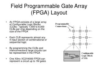
The GILES CAD Flow # Logic block parameters subblocks_per_clb 1 # 1 BLE per logic cluster subblock_lut_size 4 # 4-input LUTs # Logic block inputs and outputs inpin class: 0 bottom inpin class: 0 left inpin class: 0 top inpin class: 0 right outpin class: 1 bottom # Logic block output inpin class: 2 global left # Clock input # Connection block flexibilities Fc_type fractional # Specified as fractional number of tracks Fc_input 0.5625 # Flexibility of input connection block Fc_output 1 # Flexibility of output connection block Fc_pad 1 # Flexibility of I/O pads # Switch types switch 0 buffered: no ... switch 1 buffered: yes ... # Length 4 routing tracks, half buffered segment frequency: 0.5 length: 4 wire_switch: 0 ... segment frequency: 0.5 length: 4 wire_switch: 1 ...
Summary • Chip made in 0.18 um process • 358,374 transistors • Significant time savings • 34 person-weeks vs. > 50 person-years
Future Directions • Further automate FPGA design • Transistor sizing