Download
1 / 64
650 likes | 803 Views
From Combinational to Sequential Circuits to Simple Processors. What we covered on Friday meeting?. Design of SOP circuits from KMaps. Prime implicants and Covering Design of POS circuits from KMaps. Prime implicates and Covering

E N D
From Combinational to Sequential Circuits to Simple Processors
What we covered on Friday meeting? • Design of SOP circuits from KMaps. Prime implicants and Covering • Design of POS circuits from KMaps. Prime implicates and Covering • Design of ESOP circuits from KMaps. Algebraic rules for AND/EXOR logic. • Design using NAND and NOR gates. De Morgan Rules. • Factorization. • Multiplexers. • Iterative circuits and their types. • Using State Machines to design one-directional iterative circuits • Predicates • Oracles • SAT oracles • Graph Coloring oracles and distributed processors • SEND+MORE=MONEY problem and its oracle. • The idea of Constraint Satisfaction and Distributed Software/hardware for it. Ask questions to Mr Parasa and Mr Mathias Sunardi who actively participated.
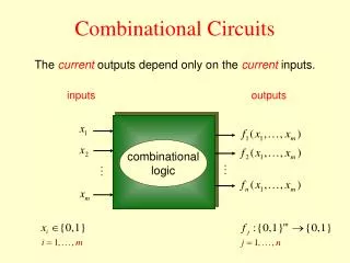
Outline • Introduction • Combinational logic • Sequential logic • FSM design • Custom single-purpose processor design • RT-level custom single-purpose processor design
Increasing abstraction level in design specification Higher abstraction level focus of hardware/software design evolution Description smaller/easier to capture E.g., Line of sequential program code can translate to 1000 gates Many more possible implementations available (a) Like flashlight, the higher above the ground, the more ground illuminated Sequential program designs may differ in performance/transistor count by orders of magnitude Logic-level designs may differ by only power of 2 (b) Design process proceeds to lower abstraction level, narrowing in on single implementation idea idea back-of-the-envelope modeling cost increases opportunities decrease sequential program register-transfers logic implementation implementation (b) (a) 5
What is Synthesis Automatically converting system’s behavioral description to a structural implementation Complex whole formed by parts Structural implementation must optimize design metrics More expensive, complex than compilers Cost = $100s to $10,000s User controls 100s of synthesis options Optimization critical Otherwise could use software Optimizations different for each user Run time = hours, days 6
Gajski’s Y-chart Each axis represents type of description Behavioral Defines outputs as function of inputs Algorithms but no implementation Structural Implements behavior by connecting components with known behavior Physical Gives size/locations of components and wires on chip/board Synthesis converts behavior at given level to structure at same level or lower E.g., FSM → gates, flip-flops (same level) FSM → transistors (lower level) FSM X registers, FUs (higher level) FSM X processors, memories (higher level) Behavior Structural Processors, memories Sequential programs Registers, FUs, MUXs Register transfers Gates, flip-flops Logic equations/FSM Transistors Transfer functions Cell Layout Modules Chips Boards Physical FU = functional unit FSM = finite state machine 7
Digital camera chip CCD CCD preprocessor Pixel coprocessor D2A A2D lens JPEG codec Microcontroller Multiplier/Accum DMA controller Display ctrl Memory controller ISA bus interface UART LCD ctrl Introduction • Processor • Digital circuit that performs a computation tasks • Controller and datapath • General-purpose: variety of computation tasks • Single-purpose: one particular computation task • Custom single-purpose: non-standard task • A custom single-purpose processor may be • Fast, small, low power • But, high NRE, longer time-to-market, less flexible
source gate Conducts if gate=1 drain 1 gate oxide IC package IC source channel drain Silicon substrate CMOS transistor on silicon • Transistor • The basic electrical component in digital systems • Acts as an on/off switch • Voltage at “gate” controls whether current flows from source to drain • Don’t confuse this “gate” with a logic gate
source source gate Conducts if gate=0 gate Conducts if gate=1 drain drain pMOS nMOS 1 1 1 x x y x F = x' y F = (xy)' x F = (x+y)' y 0 x y 0 0 NOR gate inverter NAND gate CMOS transistor implementations • Complementary Metal Oxide Semiconductor • We refer to logic levels • Typically 0 is 0V, 1 is 5V • Two basic CMOS types • nMOS conducts if gate=1 • pMOS conducts if gate=0 • Hence “complementary” • Basic gates • Inverter, NAND, NOR
x x F F x x x F F y x F x x x x x x y y y y y y F F F F F F y 0 0 0 1 F y 0 0 0 0 0 0 0 0 0 0 0 0 1 0 1 0 0 1 1 1 1 0 0 0 0 0 0 0 1 1 1 1 1 1 0 1 1 0 0 1 1 1 1 1 1 1 0 0 0 0 0 0 1 1 0 0 1 0 1 1 1 1 1 1 1 1 1 1 1 1 0 0 1 1 0 1 x x x F x F F F y y y F = x y XNOR Basic logic gates F = x Driver F = x y AND F = x + y OR F = x y XOR F = x’ Inverter F = (x y)’ NAND F = (x+y)’ NOR
B) Truth table C) Output equations D) Minimized output equations Outputs Inputs y bc y = a'bc + ab'c' + ab'c + abc' + abc a b c y z 00 01 11 10 a 0 0 0 1 0 0 0 0 0 0 0 0 1 0 1 1 1 1 1 1 z = a'b'c + a'bc' + ab'c + abc' + abc 0 1 0 0 1 0 1 1 1 0 y = a + bc z 1 0 0 1 0 bc 00 01 11 10 1 0 1 1 1 a 0 0 1 0 1 1 1 0 1 1 1 1 1 1 1 1 0 1 1 1 E) Logic Gates z = ab + b’c + bc’ a y b c z Combinational logic design A) Problem description y is 1 if a is to 1, or b and c are 1. z is 1 if b or c is to 1, but not both, or if all are 1.
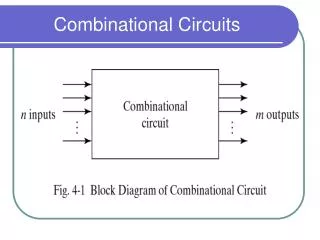
A B I1 I0 I(m-1) n n n … n bit, m function ALU S0 n-bit, m x 1 Multiplexor S0 … … S(log m) n S(log m) n O O O = I0 if S=0..00 I1 if S=0..01 … I(m-1) if S=1..11 less = 1 if A<B equal =1 if A=B greater=1 if A>B O = A op B op determined by S. O0 =1 if I=0..00 O1 =1 if I=0..01 … O(n-1) =1 if I=1..11 sum = A+B (first n bits) carry = (n+1)’th bit of A+B A B I0 A I(log n -1) B n n … n log n x n Decoder n-bit Adder n-bit Comparator With enable input e all O’s are 0 if e=0 With carry-in input Ci sum = A + B + Ci May have status outputs carry, zero, etc. … n O(n-1) O1 O0 carry sum less equal greater Combinational components
Logic synthesis Logic-level behavior to structural implementation Logic equations and/or FSM to connected gates Combinational logic synthesis Two-level minimization (Sum of products/product of sums) Best possible performance Longest path = 2 gates (AND gate + OR gate/OR gate + AND gate) Minimize size Minimum cover Minimum cover that is prime Heuristics Multilevel minimization Trade performance for size Pareto-optimal solution Heuristics FSM synthesis State minimization State encoding 14
Two-level minimization Represent logic function as sum of products (or product of sums) AND gate for each product OR gate for each sum Gives best possible performance At most 2 gate delay Goal: minimize size Minimum cover Minimum # of AND gates (sum of products) Minimum cover that is prime Minimum # of inputs to each AND gate (sum of products) Sum of products F = abc'd' + a'b'cd + a'bcd + ab'cd a b c F d Direct implementation 4 4-input AND gates and 1 4-input OR gate →40 transistors 15
Minimum cover Minimum # of AND gates (sum of products) Literal: variable or its complement a or a’, b or b’, etc. Minterm: product of literals Each literal appears exactly once abc’d’, ab’cd, a’bcd, etc. Implicant: product of literals Each literal appears no more than once abc’d’, a’cd, etc. Covers 1 or more minterms a’cd covers a’bcd and a’b’cd Cover: set of implicants that covers all minterms of function Minimum cover: cover with minimum # of implicants 16
Minimum cover: K-map approach Karnaugh map (K-map) 1 represents minterm Circle represents implicant Minimum cover Covering all 1’s with min # of circles Example: direct vs. min cover Less gates 4 vs. 5 Less transistors 28 vs. 40 cd ab 00 01 11 10 0 0 1 0 00 0 0 1 0 01 1 0 0 0 11 0 0 1 0 10 cd ab 00 01 11 10 0 0 1 0 00 0 0 1 0 01 1 0 0 0 11 0 0 1 0 10 a b F c d K-map: sum of products K-map: minimum cover Minimum cover F=abc'd' + a'cd + ab'cd Minimum cover implementation 2 4-input AND gate 1 3-input AND gates 1 4 input OR gate →28 transistors 17
Minimum cover that is prime Minimum # of inputs to AND gates Prime implicant Implicant not covered by any other implicant Max-sized circle in K-map Minimum cover that is prime Covering with min # of prime implicants Min # of max-sized circles Example: prime cover vs. min cover Same # of gates 4 vs. 4 Less transistors 26 vs. 28 K-map: minimum cover that is prime cd ab 00 01 11 10 0 0 1 0 00 0 0 1 0 01 1 0 0 0 11 Minimum cover that is prime 0 0 1 0 10 F=abc'd' + a'cd + b'cd a b F c Implementation d 1 4-input AND gate 2 3-input AND gates 1 4 input OR gate →26 transistors 18
Minimum cover: heuristics K-maps give optimal solution every time Functions with > 6 inputs too complicated Use computer-based tabular method Finds all prime implicants Finds min cover that is prime Also optimal solution every time Problem: 2n minterms for n inputs 32 inputs = 4 billion minterms Exponential complexity Heuristic Solution technique where optimal solution not guaranteed Hopefully comes close 19
Heuristics: iterative improvement Start with initial solution i.e., original logic equation Repeatedly make modifications toward better solution Common modifications Expand Replace each nonprime implicant with a prime implicant covering it Delete all implicants covered by new prime implicant Reduce Opposite of expand Reshape Expands one implicant while reducing another Maintains total # of implicants Irredundant Selects min # of implicants that cover from existing implicants Synthesis tools differ in modifications used and the order they are used 20
Multilevel logic minimization Trade performance for size Increase delay for lower # of gates Gray area represents all possible solutions Circle with X represents ideal solution Generally not possible 2-level gives best performance max delay = 2 gates Solve for smallest size Multilevel gives pareto-optimal solution Minimum delay for a given size Minimum size for a given delay multi-level minim. delay 2-level minim. size 21
Example of logic factorization Minimized 2-level logic function: F = adef + bdef + cdef + gh Requires 5 gates with 18 total gate inputs 4 ANDS and 1 OR After algebraic manipulation: F = (a + b + c)def + gh Requires only 4 gates with 11 total gate inputs 2 ANDS and 2 ORs Less inputs per gate Assume gate inputs = 2 transistors Reduced by 14 transistors 36 (18 * 2) down to 22 (11 * 2) Sacrifices performance for size Inputs a, b, and c now have 3-gate delay Iterative improvement heuristic commonly used 2-level minimized a d b e F c f g h multilevel minimized a b c d e f F g h 22
FSM synthesis FSM to gates State minimization Reduce # of states Identify and merge equivalent states Outputs, next states same for all possible inputs Tabular method gives exact solution Table of all possible state pairs If n states, n2 table entries Thus, heuristics used with large # of states State encoding Unique bit sequence for each state If n states, log2(n) bits n! possible encodings Thus, heuristics common 23
I n load shift n-bit Register n-bit Shift register n-bit Counter clear I Q n n Q Q Sequential components Q = lsb - Content shifted - I stored in msb Q = 0 if clear=1, I if load=1 and clock=1, Q(previous) otherwise. Q = 0 if clear=1, Q(prev)+1 if count=1 and clock=1. Reversible shifter shifts left and rigth Reversible counter counts up and down Reading it operation in most of registers – generalized registers.
D) State Table (Moore-type) C) Implementation Model B) State Diagram Outputs Inputs Q1 Q0 a I1 I0 x x a Combinational logic 0 0 0 0 0 x=1 x=0 a=0 a=0 0 I1 0 0 1 0 1 0 3 a=1 0 1 0 0 1 I0 0 0 1 1 1 0 a=1 a=1 1 0 0 1 0 0 Q1 Q0 1 0 1 1 1 1 2 1 1 0 1 1 1 a=1 1 1 1 0 0 State register a=0 a=0 x=0 x=0 I0 I1 Sequential logic design • Given this implementation model • Sequential logic design quickly reduces to combinational logic design A) Problem Description You want to construct a clock divider. Slow down your pre-existing clock so that you output a 1 for every four clock cycles
E) Minimized Output Equations F) Combinational Logic Q1Q0 I1 00 01 11 10 a 0 0 1 1 a 0 I1 = Q1’Q0a + Q1a’ + Q1Q0’ x 0 1 0 1 1 Q1Q0 I0 00 01 11 10 a 0 1 1 0 I1 0 I0 = Q0a’ + Q0’a 1 0 0 1 1 x I0 Q1Q0 00 01 11 10 a 0 0 1 0 x = Q1Q0 0 0 0 1 0 Q1 Q0 1 Sequential logic design (cont.)
… … external control inputs external data inputs controller datapath … … registers datapath control inputs next-state and control logic controller datapath datapath control outputs functional units state register … … external control outputs external data outputs … … a view inside the controller and datapath controller and datapath Custom single-purpose processor basic model
!1 1: (a) black-box view 1 !(!go_i) 2: !go_i x_i GCD go_i y_i 2-J: 3: x = x_i d_o 4: y = y_i !(x!=y) 5: x!=y 6: x<y !(x<y) y = y -x x = x - y 7: 8: 6-J: 5-J: d_o = x 9: 1-J: Example: greatest common divisor • First create algorithm • Convert algorithm to “complex” state machine • Known as FSMD:finite-state machine with datapath • Can use templates to perform such conversion (c) state diagram (b) desired functionality 0: int x, y; 1: while (1) { 2: while (!go_i); 3: x = x_i; 4: y = y_i; 5: while (x != y) { 6: if (x < y) 7: y = y - x; else 8: x = x - y; } 9: d_o = x; }
Assignment statement Loop statement Branch statement a = b next statement while (cond) { loop-body- statements } next statement if (c1) c1 stmts else if c2 c2 stmts else other stmts next statement !cond a = b C: C: c1 !c1*!c2 !c1*c2 cond next statement c1 stmts c2 stmts others loop-body- statements J: J: next statement next statement State diagram templates
!1 1: 1 !(!go_i) 2: x_i y_i !go_i Datapath 2-J: x_sel n-bit 2x1 n-bit 2x1 3: x = x_i y_sel x_ld 0: x 0: y 4: y = y_i y_ld !(x!=y) 5: != < subtractor subtractor x!=y 5: x!=y 5: x!=y 6: x<y 8: x-y 7: y-x 6: x_neq_y x<y !(x<y) x_lt_y 9: d y = y -x x = x - y 7: 8: d_ld d_o 6-J: 5-J: d_o = x 9: 1-J: Creating the datapath • Create a register for any declared variable • Create a functional unit for each arithmetic operation • Connect the ports, registers and functional units • Based on reads and writes • Use multiplexors for multiple sources • Create unique identifier • for each datapath component control input and output
!1 go_i 1: Controller !1 1 !(!go_i) 1: 0000 2: 1 !(!go_i) 0001 2: x_i y_i !go_i !go_i Datapath 2-J: 0010 2-J: x_sel n-bit 2x1 n-bit 2x1 3: x = x_i x_sel = 0 x_ld = 1 0011 3: y_sel x_ld 0: x 0: y 4: y = y_i y_sel = 0 y_ld = 1 y_ld 0100 4: !(x!=y) 5: !x_neq_y 0101 5: != < subtractor subtractor x!=y x_neq_y 5: x!=y 5: x!=y 6: x<y 8: x-y 7: y-x 6: 0110 6: x_neq_y x<y !(x<y) x_lt_y !x_lt_y x_lt_y 9: d y = y -x x = x - y y_sel = 1 y_ld = 1 x_sel = 1 x_ld = 1 7: 8: 7: 8: d_ld 0111 1000 d_o 6-J: 1001 6-J: 5-J: 1010 5-J: d_o = x 9: d_ld = 1 1011 9: 1-J: 1100 1-J: Creating the controller’s FSM • Same structure as FSMD • Replace complex actions/conditions with datapath configurations
x_i y_i (b) Datapath x_sel n-bit 2x1 n-bit 2x1 y_sel x_ld 0: x 0: y y_ld != < subtractor subtractor Controller implementation model 5: x!=y 5: x!=y 6: x<y 8: x-y 7: y-x go_i x_neq_y x_sel Combinational logic y_sel x_lt_y 9: d x_ld d_ld y_ld d_o x_neq_y x_lt_y d_ld Q3 Q2 Q1 Q0 State register I3 I2 I1 I0 Splitting into a controller and datapath go_i Controller !1 1: 0000 1 !(!go_i) 0001 2: !go_i 0010 2-J: x_sel = 0 x_ld = 1 0011 3: y_sel = 0 y_ld = 1 0100 4: x_neq_y=0 0101 5: x_neq_y=1 0110 6: x_lt_y=1 x_lt_y=0 y_sel = 1 y_ld = 1 x_sel = 1 x_ld = 1 7: 8: 0111 1000 1001 6-J: 1010 5-J: d_ld = 1 1011 9: 1100 1-J:
Inputs Outputs Q3 Q2 Q1 Q0 x_neq_y x_lt_y go_i I3 I2 I1 I0 x_sel y_sel x_ld y_ld d_ld 0 0 0 0 * * * 0 0 0 1 X X 0 0 0 0 0 0 1 * * 0 0 0 1 0 X X 0 0 0 0 0 0 1 * * 1 0 0 1 1 X X 0 0 0 0 0 1 0 * * * 0 0 0 1 X X 0 0 0 0 0 1 1 * * * 0 1 0 0 0 X 1 0 0 0 1 0 0 * * * 0 1 0 1 X 0 0 1 0 0 1 0 1 0 * * 1 0 1 1 X X 0 0 0 0 1 0 1 1 * * 0 1 1 0 X X 0 0 0 0 1 1 0 * 0 * 1 0 0 0 X X 0 0 0 0 1 1 0 * 1 * 0 1 1 1 X X 0 0 0 0 1 1 1 * * * 1 0 0 1 X 1 0 1 0 1 0 0 0 * * * 1 0 0 1 1 X 1 0 0 1 0 0 1 * * * 1 0 1 0 X X 0 0 0 1 0 1 0 * * * 0 1 0 1 X X 0 0 0 1 0 1 1 * * * 1 1 0 0 X X 0 0 1 1 1 0 0 * * * 0 0 0 0 X X 0 0 0 1 1 0 1 * * * 0 0 0 0 X X 0 0 0 1 1 1 0 * * * 0 0 0 0 X X 0 0 0 1 1 1 1 * * * 0 0 0 0 X X 0 0 0 Controller state table for the GCD example
… … controller datapath registers next-state and control logic functional units state register … … a view inside the controller and datapath Completing the GCD custom single-purpose processor design • We finished the datapath • We have a state table for the next state and control logic • All that’s left is combinational logic design • This is not an optimized design, but we see the basic steps You may be asked in homeworks or exams or projects to optimize the design with some respect such as area, speed , power or testability
Sender Bridge A single-purpose processor that converts two 4-bit inputs, arriving one at a time over data_in along with a rdy_in pulse, into one 8-bit output on data_out along with a rdy_out pulse. Receiver rdy_in rdy_out Problem Specification clock data_in(4) data_out(8) Bridge rdy_in=0 rdy_in=1 rdy_in=1 WaitFirst4 RecFirst4Start data_lo=data_in RecFirst4End rdy_in=0 rdy_in=0 rdy_in=1 rdy_in=1 WaitSecond4 RecSecond4Start data_hi=data_in RecSecond4End FSMD rdy_in=0 Inputs rdy_in: bit; data_in: bit[4]; Outputs rdy_out: bit; data_out:bit[8] Variables data_lo, data_hi: bit[4]; Send8Start data_out=data_hi & data_lo rdy_out=1 Send8End rdy_out=0 RT-level custom single-purpose processor design – Example “Bus Bridge” • We often start with a state machine • Rather than algorithm • Cycle timing often too central to functionality • Example • Bus bridge that converts 4-bit bus to 8-bit bus • Start with FSMD • Known as register-transfer (RT) level • Exercise: complete the design
RT-level custom single-purpose processor design (cont’) Bridge (a) Controller rdy_in=0 rdy_in=1 rdy_in=1 rdy_in rdy_out WaitFirst4 RecFirst4Start data_lo_ld=1 RecFirst4End clk data_in(4) data_out data_hi data_lo to all registers data_lo_ld data_hi_ld data_out_ld data_out rdy_in=0 rdy_in=0 (b) Datapath rdy_in=1 rdy_in=1 WaitSecond4 RecSecond4Start data_hi_ld=1 RecSecond4End Send8Start data_out_ld=1 rdy_out=1 Send8End rdy_out=0 Example “Bus Bridge”
Optimizing single-purpose processors • Optimization is the task of making design metric values the best possible • Optimization opportunities • original program • FSMD • datapath • FSM
Optimizing the original program • Analyze program attributes and look for areas of possible improvement • number of computations • size of variable • time and space complexity • operations used • multiplication and division very expensive
Optimizing the original program (cont’) original program optimized program 0: int x, y; 1: while (1) { 2: while (!go_i); 3: x = x_i; 4: y = y_i; 5: while (x != y) { 6: if (x < y) 7: y = y - x; else 8: x = x - y; } 9: d_o = x; } 0: int x, y, r; 1: while (1) { 2: while (!go_i); // x must be the larger number 3: if (x_i >= y_i) { 4: x=x_i; 5: y=y_i; } 6: else { 7: x=y_i; 8: y=x_i; } 9: while (y != 0) { 10: r = x % y; 11: x = y; 12: y = r; } 13: d_o = x; } replace the subtraction operation(s) with modulo operation in order to speed up program GCD(42, 8) - 9 iterations to complete the loop x and y values evaluated as follows : (42, 8), (43, 8), (26,8), (18,8), (10, 8), (2,8), (2,6), (2,4), (2,2). GCD(42,8) - 3 iterations to complete the loop x and y values evaluated as follows: (42, 8), (8,2), (2,0)
Optimizing the FSMD • Areas of possible improvements • merge states • states with constants on transitions can be eliminated, transition taken is already known • states with independent operations can be merged • separate states • states which require complex operations (a*b*c*d) can be broken into smaller states to reduce hardware size • scheduling
Optimizing the FSMD (cont.) int x, y; optimized FSMD !1 original FSMD 1: int x, y; 1 eliminate state 1 – transitions have constant values !(!go_i) 2: 2: go_i !go_i !go_i x = x_i y = y_i 2-J: 3: merge state 2 and state 2J – no loop operation in between them x = x_i 3: 5: 4: y = y_i x<y x>y merge state 3 and state 4 – assignment operations are independent of one another y = y -x 8: x = x - y 7: !(x!=y) 5: x!=y 9: d_o = x merge state 5 and state 6 – transitions from state 6 can be done in state 5 6: x<y !(x<y) y = y -x x = x - y 8: 7: eliminate state 5J and 6J – transitions from each state can be done from state 7 and state 8, respectively 6-J: 5-J: eliminate state 1-J – transition from state 1-J can be done directly from state 9 d_o = x 9: 1-J:
Optimizing the datapath • Sharing of functional units • one-to-one mapping, as done previously, is not necessary • if same operation occurs in different states, they can share a single functional unit • Multi-functional units • ALUs support a variety of operations, it can be shared among operations occurring in different states
Optimizing the FSM • State encoding • task of assigning a unique bit pattern to each state in an FSM • size of state register and combinational logic vary • can be treated as an ordering problem • State minimization • task of merging equivalent states into a single state • state equivalent if for all possible input combinations the two states generate the same outputs and transitions to the next same state
Technology mapping Library of gates available for implementation Simple only 2-input AND,OR gates Complex various-input AND,OR,NAND,NOR,etc. gates Efficiently implemented meta-gates (i.e., AND-OR-INVERT,MUX) Final structure consists of specified library’s components only If technology mapping integrated with logic synthesis More efficient circuit More complex problem Heuristics required 44
Complexity impact on user As complexity grows, heuristics used Heuristics differ tremendously among synthesis tools Computationally expensive Higher quality results Variable optimization effort settings Long run times (hours, days) Requires huge amounts of memory Typically needs to run on servers, workstations Fast heuristics Lower quality results Shorter run times (minutes, hours) Smaller amount of memory required Could run on PC Super-linear-time (i.e. n3) heuristics usually used User can partition large systems to reduce run times/size 1003 > 503 + 503 (1,000,000 > 250,000) 45
Integrating logic design and physical design Past Gate delay much greater than wire delay Thus, performance evaluated as # of levels of gates only Today Gate delay shrinking as feature size shrinking Wire delay increasing Performance evaluation needs wire length Transistor placement (needed for wire length) domain of physical design Thus, simultaneous logic synthesis and physical design required for efficient circuits Wire Transistor Delay Reduced feature size 46
Embedded Systems CaseStudy Elevator Controller 47
Elevator System CRC cards is a well-known method for analyzing a system and developing an architecture. CRC Classes: logical groupings of data and functionality Responsibilities: describe what the class do Collaborators: other classes w/ which a given class works Elevator Control Classes Elevator car, Passenger, Floor control, Car control, Car sensors, etc. Architectural Classes Car state, Floor control reader, Car control reader, Car control sender, Scheduler 49
F floors N hoistways 50