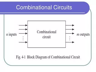
Combinational Circuits
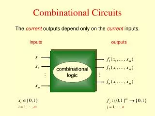
Combinational Circuits. Combinatorial. Logic. Circuit. m Boolean Inputs. n Boolean Outputs. A combinational logic circuit has: A set of m Boolean inputs, A set of n Boolean outputs, and

Combinational Circuits
E N D
Presentation Transcript
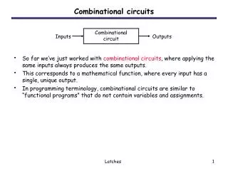
Combinational Circuits Combinatorial Logic Circuit m Boolean Inputs n Boolean Outputs • A combinational logic circuit has: • A set of m Boolean inputs, • A set of n Boolean outputs, and • n switching functions, each mapping the 2m input combinations to an output such that the current output depends only on the current input values • A block diagram:
Design Procedure • Specification • Write a specification for the circuit if one is not already available • Formulation • Derive a truth table or initial Boolean equations that define the required relationships between the inputs and outputs, if not in the specification • Apply hierarchical design if appropriate • Optimization • Apply 2-level and multiple-level optimization • Draw a logic diagram or provide a netlist for the resulting circuit using ANDs, ORs, and inverters
Design Procedure • Technology Mapping • Map the logic diagram or netlist to the implementation technology selected • Verification • Verify the correctness of the final design manually or using simulation
Design Example • Specification • BCD to Excess-3 code converter • Transforms BCD code for the decimal digits to Excess-3 code for the decimal digits • BCD code words for digits 0 through 9: 4-bit patterns 0000 to 1001, respectively • Excess-3 code words for digits 0 through 9: 4-bit patterns consisting of 3 (binary 0011) added to each BCD code word • Implementation: • multiple-level circuit • NAND gates (including inverters)
Design Example (continued) • Formulation • Conversion of 4-bit codes can be most easily formulated by a truth table • Variables- BCD: A,B,C,D • Variables- Excess-3 W,X,Y,Z • Don’t Cares- BCD 1010 to 1111
Design Example (continued) C C z y 1 1 1 1 0 1 3 2 0 1 3 2 1 1 1 1 4 5 7 6 4 5 7 6 B B X X X X X X X X 12 13 15 14 12 13 15 14 A A 1 X X 1 X X 8 9 11 10 8 9 11 10 D D D D x C C w 1 1 1 0 1 3 2 0 1 3 2 1 1 1 1 4 5 7 6 4 5 7 6 B B X X X X X X X X 12 13 15 14 12 13 15 14 A A 1 X X 1 1 X X 8 9 11 10 8 9 11 10 D B C B C D D • Optimization • 2-level usingK-maps W = A + BC + BD X = C + D + B Y = CD + Z =
Design Example (continued) B B C C D D D D D D B C C • Optimization (continued) • Multiple-level using transformationsW = A + BC + BD X = C + D + BY = CD + Z = G = 7 + 10 + 6 + 0 = 23 • Perform extraction, finding factor: T1 = C + DW = A + BT1X = T1 + BY = CD + Z = G = 2 + 1 + 4 + 7 + 6 + 0 = 19
Design Example (continued) B B C D D D D D C T1 T1 T1 C • Optimization (continued) • Multiple-level using transformationsT1 = C + DW = A + BT1X = T1 + BY = CD + Z = G = 19 • An additional extraction not shown in the text since it uses a Boolean transformation: ( = C + D = ): W = A + BT1X = T1 + B Y = CD + Z = G = 2 +1 + 4 + 6 + 4 + 0 = 16!
Design Example (continued) A W B X Y C D Z • Technology Mapping • Mapping with a library containing inverters and 2-input NAND, 2-input NOR, and 2-2 AOI gates
Beginning Hierarchical Design • To control the complexity of the function mapping inputs to outputs: • Decompose the function into smaller pieces called blocks • Decompose each block’s function into smaller blocks, repeating as necessary until all blocks are small enough • Any block not decomposed is called a primitive block • The collection of all blocks including the decomposed ones is a hierarchy • Example: 9-input parity tree (see next slide) • Top Level: 9 inputs, one output • 2nd Level: Four 3-bit odd parity trees in two levels • 3rd Level: Two 2-bit exclusive-OR functions • Primitives: Four 2-input NAND gates • Design requires 4 X 2 X 4 = 32 2-input NAND gates
Hierarchy for Parity Tree Example X 0 X 1 X 2 9-Input X 3 odd X Z O 4 X function 5 X X A 6 0 0 3-Input X 7 odd A X B X 1 8 O 1 function A X (a) Symbol for circuit 2 2 X A A 3 0 0 3-Input 3-Input odd odd A A X B Z B 1 1 4 O O O function function A A X 2 2 5 X A 6 0 3-Input odd A X B 1 7 O function A X 2 8 (b) Circuit as interconnected 3-input odd function blocks A 0 A B 1 O A 2 (c) 3-input odd function circuit as interconnected exclusive-OR blocks (d) Exclusive-OR block as interconnected NANDs
Reusable Functions • Whenever possible, we try to decompose a complex design into common, reusable function blocks • These blocks are • verified and well-documented • placed in libraries for future use
Top-Down versus Bottom-Up • A top-down design proceeds from an abstract, high-level specification to a more and more detailed design by decomposition and successive refinement • A bottom-up design starts with detailed primitive blocks and combines them into larger and more complex functional blocks • Design usually proceeds top-down to known building blocks ranging from complete CPUs to primitive logic gates or electronic components. • Much of the material in this chapter is devoted to learning about combinational blocks used in top-down design.
Technology Mapping • Mapping Procedures • To NAND gates • To NOR gates • Mapping to multiple types of logic blocks in covered in the reading supplement: Advanced Technology Mapping.
Mapping to NAND gates • Assumptions: • Gate loading and delay are ignored • Cell library contains an inverter and n-input NAND gates, n = 2, 3, … • An AND, OR, inverter schematic for the circuit is available • The mapping is accomplished by: • Replacing AND and OR symbols, • Pushing inverters through circuit fan-out points, and • Canceling inverter pairs
NAND Mapping Algorithm • Replace ANDs and ORs: • Repeat the following pair of actions until there is at most one inverter between : • A circuit input or driving NAND gate output, and • The attached NAND gate inputs.
Mapping to NOR gates • Assumptions: • Gate loading and delay are ignored • Cell library contains an inverter and n-input NOR gates, n = 2, 3, … • An AND, OR, inverter schematic for the circuit is available • The mapping is accomplished by: • Replacing AND and OR symbols, • Pushing inverters through circuit fan-out points, and • Canceling inverter pairs
NOR Mapping Algorithm • Replace ANDs and ORs: • Repeat the following pair of actions until there is at most one inverter between : • A circuit input or driving NAND gate output, and • The attached NAND gate inputs.
NOR Mapping Example A A B B 2 X 1 F C F C 3 D D E E A (a) (b) B C F D E (c)
Verification • Verification - show that the final circuit designed implements the original specification • Simple specifications are: • truth tables • Boolean equations • HDL code • If the above result from formulation and are not the original specification, it is critical that the formulation process be flawless for the verification to be valid!
Basic Verification Methods • Manual Logic Analysis • Find the truth table or Boolean equations for the final circuit • Compare the final circuit truth table with the specified truth table, or • Show that the Boolean equations for the final circuit are equal to the specified Boolean equations • Simulation • Simulate the final circuit (or its netlist, possibly written as an HDL) and the specified truth table, equations, or HDL description using test input values that fully validate correctness. • The obvious test for a combinational circuit is application of all possible “care” input combinations from the specification
Verification Example: Simulation • Simulation procedure: • Use a schematic editor or text editor to enter a gate level representation of the final circuit • Use a waveform editor or text editor to enter a test consisting of a sequence of input combinations to be applied to the circuit • This test should guarantee the correctness of the circuit if the simulated responses to it are correct • Short of applying all possible “care” input combinations, generation of such a test can be difficult
Verification Example: Simulation • Enter BCD-to-Excess-3 Code Converter Circuit Schematic AOI symbolnot available
Verification Example: Simulation • Enter waveform that applies all possible input combinations: • Are all BCD input combinations present? (Low is a 0 and high is a one)
Verification Example: Simulation • Run the simulation of the circuit for 120 ns • Do the simulation output combinations match the original truth table?
Functions and Functional Blocks • The functions considered are those found to be very useful in design • Corresponding to each of the functions is a combinational circuit implementation called a functional block. • In the past, functional blocks were packaged as small-scale-integrated (SSI), medium-scale integrated (MSI), and large-scale-integrated (LSI) circuits. • Today, they are often simply implemented within a very-large-scale-integrated (VLSI) circuit.
Rudimentary Logic Functions • Functions of a single variable X • Can be used on theinputs to functionalblocks to implementother than the block’sintended function T A BLE 4-1 Functions of One V a ria b le X F = 0 F = X F = X F = 1 0 0 0 1 1 1 0 1 0 1
Multiple-bit Rudimentary Functions A A • Multi-bit Examples: • A wide line is used to representa bus which is a vector signal • In (b) of the example, F = (F3, F2, F1, F0) is a bus. • The bus can be split into individual bits as shown in (b) • Sets of bits can be split from the bus as shown in (c)for bits 2 and 1 of F. • The sets of bits need not be continuous as shown in (d) for bits 3, 1, and 0 of F. F 3 2 3 1 2:1 F(2:1) 2 F 1 4 4 2 F F 0 0 F 1 1 0 (c) A A F 0 3 (a) (b) 3,1:0 F(3), F(1:0) 4 F (d)
Enabling Function • Enabling permits an input signal to pass through to an output • Disabling blocks an input signal from passing through to an output, replacing it with a fixed value • The value on the output when it is disable can be Hi-Z (as for three-state buffers and transmission gates), 0 , or 1 • When disabled, 0 output • When disabled, 1 output • See Enabling App in text
3-7 Decoding D0 D1 : : Dm-1 A0 : : An-1 m-elements ≤ 2n n-2n decoder n bits • A n-bit binary code can represent up to m=2n elements: m elements n-bit binary code • Decoding - the conversion of an n-bit input code to an m-bit output code withn ≤ m ≤ 2n such that each valid code word produces a unique output code encoding (ex. 256 alpha-num. chars) (ex. 8-bit ASCII code) decoding
Decoder examples a b c : : g a b BCD code decoder M 2 • BCD to 7-segment decoder: • Binary to ASCII. • Address decoder in a memory: Row Example: 4Mbit DRAM No. of memory positions: 222 This requires 22 address bits: N row address bits (ex. 11) M column addr bit (ex. 11) The address bits are decoded into actual memory locations 1 Decoder 1 MATRIX OF MEMORY Row address CELLS one cell N N 2 1 Column decoder Read Write Control M 1 Column address Out In Data
2-to-4 line decoder 1 0 0 0 0 1 0 0 0 0 1 0 0 0 0 1 A A D D D D 2 1 0 0 3 1 0 0 0 1 1 0 1 1 Logic expressions: D A A = 0 1 0 D A A = 1 1 0 D A A = 2 1 0 D A A = 3 1 0 Table: D0 D1 D2 D3 0 1 2 3 A0 A1 0 1 2-4 line Decoder ? only one of the inputs is active minterms
2-to-4 Line Decoder circuit D A A = 0 1 0 D A A = 1 1 0 D A A = 2 1 0 D A A = 3 1 0 A 0 A 1 Notice that the outputs of the decoder correspond to the minterms: Di=mi
Decoder Expansion • Larger decoders can be realized by implementing each minterm using a single AND gate: • However for large decoders this requires multiple input AND gates which is not always feasible. • Better to use a hierarchical approach: build larger ones from smaller decoders. • Approach: • Output AND gates have only 2 inputs and implement the minterms. • The output AND gates are driven by two decoders with their numbers of inputs either equal or differing by 1.
Decoder Expansion - Example 1 A2’A1’A0’ A2’A1’A0 A0 A1 2-4 Decoder A2’A1A0’ A1’A0 A2’A1A0 D0 D1 D2 D3 A’1A’0 A1A0 A0 A1 A’1A0 2-4 Decoder A2 A’2 A2A1’A0’ A2 AA0’ A1A0 A2A1A0 3-to-8 decoder • 3-to-8-line decoder • Number of output ANDs = 8 • Number of inputs: 3 A’1A’0 A’1A0 1-to-2 decoder
Rule for building large decoders • k-to-2k decoder: • One needs 2k output AND gates • If k can be divided by 2: • use two k/2-to-2k/2 decoders • If k cannot divided by 2: • use a (k+1)/2 and • use a (k-1)/2 decoder. • Previous example: 3-to-8 decoder (k=3): • Use a 2-to-4 and a 1-to-2 decoder
Example : build a 4-to-16 decoder • How many 2-input output AND gates? • Which smaller decoders to use? • Draw the circuit.
4-to-16 decoder A3’A2’A1’A0’ D0 D1 D2 D3 D4 : : A3’A2’A1’A0 A1’A0’ D0 D1 D2 D3 A0 A1 A1’A0 2-4 Decoder A1A0’ A3’A2’A1A0 A3’A2A1’A0’ A1A0 A3’A2’ D0 D1 D2 D3 A2 A3 A3’A2 2-4 Decoder A3A2 A3A2A1A0’ A3A2A1A0 Use two 2-to-22 decoders D14 D15
Decoder Expansion - Exercise 2 • 5-to-32-line decoder • Number of output ANDs = ? • Number of inputs to decoders driving output ANDs = ? • Which decoders to use to drive the output ANDs? • Block diagram:
5-to-32-line decoder A4’A3’ A2’A1’A0’ D0 D1 D2 D3 D4 D7 : : A2’A1’A0’ D0 D1 D2 D3 D7 A4’A3’ A2’A1’A0 A2’A1’A0 A0 A1 A2 3-8 Decoder A4’A4’ D0 D1 D2 D3 A3 A4 A3’A2 2-4 Decoder A4A3 D30 D31 A2A1A0 A4A3
Decoder Expansion - Example 2 • 7-to-128-line decoder • Number of output ANDs = ? • Number of inputs to decoders driving output ANDs = ? • Closest possible split to equal
Decoder with Enable EN D0 D1 D2 D3 A0 A1 2-4 Decoder • Extra input EN: • If EN = 1: act as a regular decoder • If EN=0, all outputs are 0 • See truth table below for function 0 1
Decoder with Enable: circuit D0 D1 D2 D3 EN=IN Demux EN D0 D1 D2 D3 A0 A1 A1 A0 2-4 Decoder EN Extra set of ands If one considers EN an input, in that case the circuit can be viewed as distributing value of signal EN(=IN) to 1 of 4 outputs: called a demultiplexer: 0 1 Regular decoder 0 1 2 3 1 0
Example: Sprinkler System • Design the sprinkler valve controller • Description: • The system has 8 different zones • Only one value is on at one time (to maintain the pressure) • A microcontroller is used to control the valves: • However the processor has only 4 outputs • Lets program the microcontroller to indicate which of the 8 valves should be opened, using a binary representation.
Sprinkler System a b c d Micro- controller • We can use a 3-to-8 decoder with enable input controlled by the microprocessor D0=A2’A1’A0’.EN D1=A2’A1’A0.EN A0 A1 A2 D0 D1 D2 D3 D7 0 1 2 3-8 Decoder D7=A2A1A0.EN EN When EN=0, all valves are off
Combinational Logic Implementation- Decoder and OR Gates • Implement m functions of n variables with: • Sum-of-minterms expressions • One n-to-2n-line decoder • mOR gates, one for each output
Example A B C F 0 0 0 0 0 0 1 0 0 1 0 0 0 1 1 1 1 0 0 0 1 0 1 1 1 1 0 1 1 1 1 1 0 1 2 3 4 5 6 7 A B C F • Design and implement a majority function F(ABC) using a 3-to-8 decoder • Truth table: • Minterms: • F=m(3,5,6,7) • Implementation using decoder: Indicate MSB, LSB 2 1 0