Combinational Circuits Overview: Chip Design and Logic
Learn about combinational circuits and crucial design concepts in chip design and logic. Explore the importance of hierarchy, reuse of blocks, integrated circuits, and technology parameters.

Combinational Circuits Overview: Chip Design and Logic
E N D
Presentation Transcript
Overview Combinational Logic • Combinational Circuit • Chip Design styles • Full-custom design • Cell library based design • Programmable Logic Array
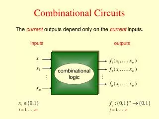
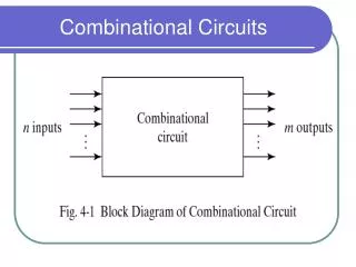
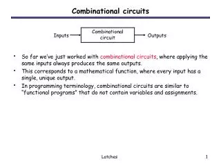
Combinational Circuits Combinational Logic A combinational circuit consists of logic gates whose outputs, at any time, are determined by combining the values of the inputs. For n input variables, there are 2n possible binary input combinations. For each binary combination of the input variables, there is one possible output.
Combinational Circuits (cont.) Combinational Circuit n-inputs m-outputs • • • • • • Combinational Logic • Hence, a combinational circuit can be described by: • A truth table that lists the output values for each combination of the input variables, or • m Boolean functions, one for each output variable.
Combinational vs. Sequential Circuits • Combinational circuits are memory-less. Thus, the output value depends ONLY on the current input values. • Sequential circuits consist of combinational logic as well as memory elements (used to store certain circuit states). Outputs depend on BOTH current input values and previous input values (kept in the storage elements). Combinational Logic
Combinational vs. Sequential Circuits Combinational Circuit n-inputs m-outputs (Depend only on inputs) Combinational Circuit n-inputs m-outputs Combinational Circuit Storage Elements Present state Next state Sequential Circuit Combinational Logic
Important Design Concepts Combinational Logic • Modern digital design deals with various methods and tools that are used to design and verify complex circuits and systems. • Concepts: • Design Hierarchy • Computer-Aided-Design (CAD) tools • Hardware Description Languages (HDLs)
Design Hierarchy Combinational Logic “Divide-and-Conquer” approach used to cope with the challenges of designing complex circuits and systems (many times in the order of millions of gates). Circuit is broken into blocks, repetitively.
Design Hierarchy To control the complexity of the function mapping inputs to outputs: *Decompose the function into smaller pieces called blocks. *Decompose each block’s function into smaller blocks, repeating as necessary until all blocks are small enough. *Any block not decomposed is called a primitive block. *The collection of all blocks including the decomposed ones is a hierarchy. Example: 9-input parity tree (see next slide) Top Level: 9 inputs, one output 2nd Level: Four 3-bit odd parity trees in two levels 3rd Level: Two 2-bit exclusive-OR functions Primitives: Four 2-input NAND gates Combinational Logic
Design Hierarchy Example: 9-input odd function (for counting # of 1 in inputs) Combinational Logic
Why is Hierarchy useful? Combinational Logic Reduces the complexity required to design and represent the overall schematic of the circuit. Reuse of blocks is possible. Identical blocks can be used in various places in a design, or in different designs.
Reusable Functions and CAD Combinational Logic • Whenever possible, we try to decompose a complex design into common, reusable function blocks • These blocks are • verified and well-documented • placed in libraries for future use
Integrated Circuits Combinational Logic • Integrated circuit (a chip) is a semiconductor crystal (most often silicon) containing the electronic components for the digital gates and storage elements which are interconnected on the chip. • Terminology - Levels of chip integration • SSI (small-scale integrated) - fewer than 10 gates • MSI (medium-scale integrated) - 10 to 100 gates • LSI (large-scale integrated) - 100 to thousands of gates • VLSI (very large-scale integrated) - thousands to 100s of millions of gates
Technology Parameters Combinational Logic • Specific gate implementation technologies are characterized by the following parameters: • Fan-in – the number of inputs available on a gate • Fan-out – the number of standard loads driven by a gate output • Cost for a gate - a measure of the contribution by the gate to the cost of the integrated circuit • Propagation Delay – The time required for a change in the value of a signal to propagate from an input to an output • Power Dissipation – the amount of power drawn from the power supply and consumed by the gate
Propagation Delay • Propagation delay is the time for a change on an input of a gate to propagate to the output. • Delay is usually measured at the 50% point with respect to the H and L output voltage levels. • High-to-low (tPHL) and low-to-high (tPLH) output signal changes may have different propagation delays. • High-to-low (HL) and low-to-high (LH) transitions are defined with respect to the output, not the input. • An HL input transition causes: • an LH output transition if the gate inverts and • an HL output transition if the gate does not invert. Combinational Logic
Propagation Delay Example IN (volts) OUT (volts) t (ns) 1.0 ns per division Combinational Logic
Chip Design Styles Combinational Logic • Full custom - the entire design of the chip down to the smallest detail of the layout is performed • Expensive, its timing and power is hard to analyze • only for dense, fast chips with high sales volume • Standard cell - blocks have been design ahead of time or as part of previous designs • Intermediate cost • Less density and speed compared to full custom • Gate array - regular patterns of gate transistors that can be used in many designs built into chip - only the interconnections between gates are specific to a design • Lowest cost • Less density compared to full custom and standard cell • Prototype design • The base of FPGA
Cell Libraries Combinational Logic Cell - a pre-designed primitive block Cell library - a collection of cells available for design using a particular implementation technology Cell characterization - a detailed specification of a cell for use by a designer
Cell Library Based Design Procedure Combinational Logic • Specification • Write a specification for the circuit if one is not already available • Formulation • Derive a truth table or initial Boolean equations that define the required relationships between the inputs and outputs, if not in the specification • Optimization • Draw a logic diagram or provide a netlist for the resulting circuit using ANDs, ORs, and inverters
Cell Library Based Design Procedure Combinational Logic • Technology Mapping • Map the logic diagram to the implementation technology selected • Map to CMOS • Evaluation • Evaluate the timing and power
Programmable Logic Array Combinational Logic The set of functions to be implemented is first transformed to product terms Since output inversion is available, terms can implement either a function or its complement
Programmable Logic Array Example Combinational Logic • To implement • F1= A’B’C+A’BC’+AB’C’=(AB+AC+BC+A’B’C’)’ • F2=AB+AC+BC
A B C X X X 1 X 2 X X X X X Fuse intact Fuse blown X X X 3 X X 4 X X X 0 X C C B B A A 1 X F 1 F 2 Programmable Logic Array Example Combinational Logic
Kingdom of Saudi Arabia Ministry of Education Umm AlQura University Adam University College Computer Science Department المملكة العربية السعودية وزارة التعليم جامعة أم القرى الكلية الجامعية أضم قسم الحاسب الآلي This Summary is an Online Content from this Book:Morris Mano, DIGITAL DESIGN, 4th Edition, Prentice Hall, 2007It is edited forLogic Analysis and Design Course 6803213-3 by:T.Mariah Sami KhayatTeacher Assistant @ Adam University CollegeFor Contacting:mskhayat@uqu.edu.sa Combinational Logic