Download
1 / 18
180 likes | 198 Views
Insights on n-XYTER front end boards, chip developments, and radiation hardness observations. Highlights from various collaborations and engineering runs. Future hybrid technology prospects and building blocks for CBM-XYTER.

E N D
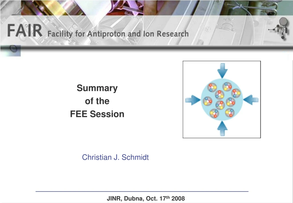
Summaryof the FEE Session Christian J. Schmidt JINR, Dubna, Oct. 17th 2008
Activities • n-XYTER front end boards and hybrid technologies • Status of the n-XYTER engineering run • CBM-Dedicated Chip Developments • Preliminary observations on radiation hardness of the chip technology (UMC 0.180) • Status of chip development work • CBM-XYTER Family Planning
"Simple" FEB for the n-XYTER Starter Kit • Allow development of the DAQ chain • Allow the readout of various detector prototypes After several iterations, technology seems to get straight: FEB-Rev D will be distributable at the end of the year! The September beam time has shown the whole signal chain operative! Silicon Strip / GEM Gas Detectors --- n-XYTER --- SysCore DAQ System
Other Versions for other applications in production 2 chips on n-XYTER-GEM (FoPi GEM-TPC) 4 chips on n-XYTER-Quattro (CBM-STS test) Rafal Lalik (AGH Krakow/GSI) has realized FEBs for several applications
Future hybrid technology, very promising options • Bump bonding may be the technology for our STS hybrid assembly! • Hybrid assembly with Si-based circuit board • very dense assemblies • cooling from both sides possible • devices may be stacked One dummy module populated with 52 chips No failures ! Christian Kreidl, ZITI Heidelberg
Activities in Heidelberg: n-XYTER engineering run preparation Engineering Run of the n-XYTER will supply chips for detector prototyping activities! Hans K.Soltveit, Physik. Inst. Heidelberg • Some modifications included: • Annoying temp. coefficient addressed • Rearrangement of bond-pads for better interconnect • Two different versions of dynamic range in one submission: 120 000 e and 1000 000 e. • Extensive simulations realized (corners analysis) • Schematics review in November 2008 • Layout review in January, submission to follow
TEMPERATURE SENSITIVITY Config. for positive input signals NEW: TEMP.COEFF. ~0.5 mV/°C Old TEMP.COEFF. ~29 mV/°C FAST-SHAPER OUTPUT DC-LEVEL Config for negative input signals NEW: TEMP.COEFF. ~0.7 mV/°C TEMP(°C) Hans K.Soltveit, Physik. Inst. Heidelberg
Radiation Hardness Tests on UMC 0.180µ single DEPFET pixel chip with many DEPFET pixels ZITI current mode logic (Ivan Peric)
Very promising observations: Damage does anneal! • Very promising observations! Valuable support from Valeriy Shunkov (Inst. for System Studies) towards modelling effects Very similar results observed by Sven Loechner GSI on test transistors
Building blocks for the CBM-XYTER at ZITI Heidelberg • Concentrated ADC expertise at ZITI • David Muthers ADC resurrected (Kaiserslautern) • New Current Mode ADC (Ivan Peric, ZITI) Design study very promising • 9 bit, 25 MHz, 4.5 mW (0.36 pJ/conv.) • Simple Serial Data Driver • Prestudy towards a serial chip data-interface • CMOS standard cells yield 1.9 GHz DEPFET Pixel with 2 ADC Size x: 180µm Size y: 110µm
Second Front End Test Chip Submitted at ZITI Heidelberg More Building blocks for the CBM-XYTER • 26 channel charge sensitive amplifier • scaling: multiple parallel amplifier cells to meet overall noise specs • study various pulse injection circuits • study current mode logic based discriminator Work by Tim Armbruster, ZiTi Heidelberg Chips expected Jan. 2009
NIHAM Bucharest: TRD Front-End Test Chip close to Submission Particular emphasis on high counting rates TRD needs • peaking times adapted to high counting rate TRD • analogue baseline restauration • particularly fast return to baseline from overload • choice of peaking time (20ns, 40ns) • fast peak detector Vasile Catanescu, NIHAM Bucharest
The Dedicated CBM-XYTER, Family Planning Common process 0.180nm UMC, on-chip infrastructure, rad. hard libraries but different architectural specifics • STS-XYTER • minimize power • dc-leakage compensation • compact, high channel density • MIP sensitivity in Si • dense mounting • 4 to 5 bit res. • TRD-XYTER • high resolution needs (8 to 9 bit) • lower channel density • next neighbor forced trigger logic? • ion tail cancellation facilities • baseline restauration • lower occupancy MUCH needs are somewhere in between. Preferably adopt these specs within one of the two! R. Szczygiel, P. Grybos AGH Krakow Realization in TOT architecure P. Fischer ZITI Uni-Heidelberg Architecture/specs not yet settled
Discussion on CBM TRD electronics needs started Mihai Petrovici, NIHAM Bucharest
Discussion on CBM MUCH electronics needs started V. Nikulin agreed to help out with thoughts on MUCH electronics needs!
Towards Specs for TRD and MUCH-XYTER • Workshop planned early Dec. 2008 • Get electronics- and detector-experts together • Work-out the architectural needs and specifications for both detectors • Principle questions to be answered: • Can we subsum MUCH and TRD electronics needs within one chip? • Specifications for the TRD-XYTER chip • Chip-System design may start from there