Download
1 / 40
420 likes | 667 Views
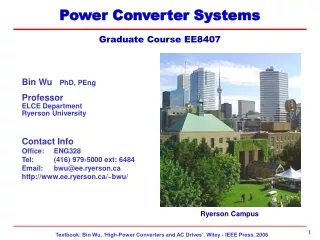
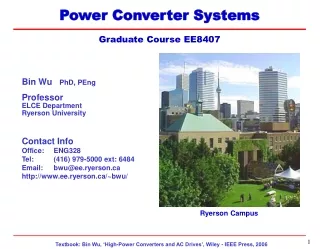
Power Converter Systems Graduate Course EE8407. Bin Wu PhD, PEng Professor ELCE Department Ryerson University Contact Info Office: ENG328 Tel: (416) 979-5000 ext: 6484 Email: bwu@ee.ryerson.ca http://www.ee.ryerson.ca/~bwu/. Ryerson Campus. Topic 5

E N D
Power Converter Systems Graduate Course EE8407 Bin Wu PhD, PEng Professor ELCE Department Ryerson University Contact Info Office: ENG328 Tel: (416) 979-5000 ext: 6484 Email: bwu@ee.ryerson.ca http://www.ee.ryerson.ca/~bwu/ Ryerson Campus
Topic 5 Two-Level Voltage Source Inverter (VSI) Source: Alstom VDM5000 Two-level VSI
Two Level Voltage Source Inverter Lecture Topics • Sinusoidal PWM • Space vector modulation Why Use PWM Techniques? • To control inverter output frequency (fundamental) • To control inverter output voltage (fundamental) • To minimize harmonic distortion
Sinusoidal PWM • Inverter Configuration Assumption: dc capacitor very large dc voltage ripple free
Sinusoidal PWM • Modulating and Carrier Waves • vcr – Carrier wave (triangle) • Amplitude modulation index • vm – Modulating wave (sine) • Frequency modulation index
Sinusoidal PWM • Gate Signal Generation Vg1 and Vg4 are complementary
Sinusoidal PWM • Line-to-Line Voltage vAB
Sinusoidal PWM • Waveforms and FFT • ma= 0.8, mf= 15, • fm= 60Hz, fcr= 900Hz • Switching frequency • fsw= fcr = 900Hz
Sinusoidal PWM • Harmonic Content • Low order harmonics • n < (mf-2) are eliminated • VAB1 versus ma is linear • VAB1,max = 0.612Vd
Sinusoidal PWM • Over-Modulation • Fundamental voltage ↑ • Low-order harmonics ↑
Sinusoidal PWM • Third Harmonic Injection PWM • - Fundamental voltage increased • - No low order harmonics produced • 3rd harmonic – zero sequence (to appear in vANandvBN ) • No triplen harmonics in vAB (vAB = vAN - vBN)
Space Vector Modulation • Switching States
Space Vector Modulation • Switching States (Three-Phase) • Eight switching states
Space Vector Modulation • Space Vector Diagram • Active vectors: to • (stationary, not rotating) • Zero vector: • Six sectors: I to VI
Space Vector Modulation • Space Vectors • Three-phase voltages (1) • Two-phase voltages (2) • Space vector representation (3) (2) (3) (4) where
Space Vector Modulation • Space Vectors (Example) Switching state [POO] S1, S6 and S2 ON and (5) (5) (4) (6) Similarly, (7)
Space Vector Modulation • Active and Zero Vectors • Active Vector: 6 • Zero Vector: 1 • Redundant switching • states: [PPP] and [OOO]
Space Vector Modulation • Reference Vector Vref • Definition • Rotating in space at ω (8) • Angular displacement (9)
Space Vector Modulation • Relationship Between Vref and VAB • Vrefis approximated by two active • and a zero vectors • Vrefrotates one revolution, • VAB completes one cycle • Length of Vref corresponds to • magnitude of VAB
Space Vector Modulation • Dwell Time Calculation • Volt-Second Balancing (10) • Ta, Tb and T0– dwell times for and • Ts– sampling period • Space vectors , and (11) (11) (10) (12)
Space Vector Modulation • Dwell Times Solve (12) (13)
Space Vector Modulation • VrefLocation versus Dwell Times
Space Vector Modulation • Modulation Index (15) (16)
Space Vector Modulation • Modulation Range • Vref,max (17) (17) (16) • ma,max= 1 • Modulation range: 0 ma 1 (18)
Space Vector Modulation • Switching Sequence Design • Basic Requirement: Minimize the number of switchings per sampling period Ts • Implementation: Transition from one switching state to the next involves only two switches in the same inverter leg.
Space Vector Modulation • Seven-segment Switching Sequence • Selected vectors: • V0, V1 and V2 • Dwell times: • Ts = T0 + Ta + Tb • Total number of switchings: 6
Space Vector Modulation • Undesirable Switching Sequence • Vectors V1 and V2 swapped • Total number of switchings: 10
Space Vector Modulation • Switching Sequence Summary (7–segments) Note: The switching sequences for the odd and ever sectors are different.
Space Vector Modulation • Simulated Waveforms f1 = 60Hz, fsw= 900Hz,ma = 0.696, Ts = 1.1ms
Space Vector Modulation • Waveforms and FFT
Space Vector Modulation • Waveforms and FFT (Measured)
Space Vector Modulation • Waveforms and FFT (Measured) ( and )
Space Vector Modulation • Even-Order Harmonic Elimination Type-A sequence (starts and ends with [OOO]) Type-B sequence (starts and ends with [PPP])
Space Vector Modulation • Even-Order Harmonic Elimination Space vector Diagram
Space Vector Modulation • Even-Order Harmonic Elimination • Measured waveforms and FFT
Space Vector Modulation • Even-Order Harmonic Elimination ( and )
Space Vector Modulation • Five-segment SVM
Space Vector Modulation • Switching Sequence ( 5-segment)
Space Vector Modulation • Simulated Waveforms ( 5-segment) • f1 = 60Hz, fsw= 600Hz, ma = 0.696, Ts = 1.1ms • No switching for a 120° period per cycle. • Low switching frequency but high harmonic distortion