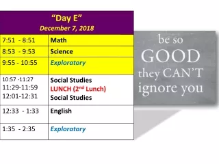
Lecture 5 Key Locker using FPGA
Lecture 5 Key Locker using FPGA. 2007/10/05 Prof. C.M. Kyung. Key Locker Design Using FPGA. 1. GOAL is ~ (1) Understanding of FSM and Its Sequential Behaviors (2) Understanding of the Design Procedure for FSM (3) Design of the FSM for Key Locker and Implementation on FPGAs.

Lecture 5 Key Locker using FPGA
E N D
Presentation Transcript
Lecture 5 Key Locker using FPGA 2007/10/05 Prof. C.M. Kyung
Key Locker Design Using FPGA • 1. GOAL is ~ • (1) Understanding of FSM and Its Sequential Behaviors • (2) Understanding of the Design Procedure for FSM • (3) Design of the FSM for Key Locker and Implementation on FPGAs
Key Locker Design Using FPGA • 2. Review of Sequential Logic Circuits • (1) Sequential Systems • - Having memory. • - The current state is “held” in memory and the next state is • computed based on the current state and the current inputs. • - Clock orchestrates the sequence of events
Key Locker Design Using FPGA • 2. Review of Sequential Logic Circuits • (1) Basic Building Blocks for Sequential Systems • - D Flip Flop • - T Flip Flop
Key Locker Design Using FPGA • 3. Design Procedure for State Machines • (1) Description of SM - State diagram, SM chart, … • (2) State Optimization • - Elimination of redundant states, … • (3) State Encoding • - Gray, One-hot, Thermometer, … • (4) Logic Minimization • - K-MAP, Quine-Mckluskey Method, … In modern design flows, these are usually done easily with CAD tools
Key Locker Design Using FPGA • 4. State Machine Design • (1) State Graph, State Table
Key Locker Design Using FPGA • 4. State Machine Design • (2) No state machine optimization • (3) State encoding
Key Locker Design Using FPGA • 4. State Machine Design • (4) Result of Logic Minimization
Key Locker Design Using FPGA • 5. Practical Design of FSM • (1) In good design, data path and control path are clearly separated
Key Locker Design Using FPGA • (2) Example description of FSM in Verilog HDL
Key Locker Design Using FPGA • (3) Timing Constraints for Sequential Logics • - Set-up time (Tsu) • Input should be “set-up” early enough before the clocking event. • - Hold time (Th) • Input should be “held” at least some time after the clocking event.
Key Locker Design Using FPGA • (4) Synchronizations of External Inputs - Bouncing • - In mechanical switching, any two metal contacts generate multiple • signals as the contacts close or open. - This should be prohibited for properly working in the digital logic circuits.
Key Locker Design Using FPGA • (5) De-bouncing Technique • - RC De-bouncer • - Flip-Flop Based De-bouncer • - Software Based De-bouncer switch signal CLK
Key Locker Design Using FPGA • 6. Problem statement • (1) Key Locker System - Given the *XXXXX* as the password input, • the electric locker will be open or not. • - Illegal password input should be handled gracefully. • - Design should be implemented and verified within EPLD.
Key Locker Design Using FPGA • 6. Problem statement • (2) Key-Pad Circuit
Key Locker Design Using FPGA • 6. Problem statement • (3) Finite State Machine for Key Locker • - Input from key-pad should be de-bounced • - For each input from the key-pad circuit, the internal state • in the FSM should be transit properly. • - Password checking including illegal password handling.
Key Locker Design Using FPGA • 7. Experiment Requirements • (1) Equipment - Breadboard- KeyLocker Machine- DC Power Supply • (2) Component • - Switch • (3) TTL IC’s • - 7400 (2 input NAND gate) • - 7404 (Inverter) • - 7408 (2 input AND gate) • - 7410 (3 input NAND gate) • - 74LS73 ( Dual J-K flip-flop ) • - 74LS74 ( Dual D-Type flip-flop )
Key Locker Design Using FPGA • 8. References • (1) Textbook • - Contemporary Logic Design - Katz • - Fundamentals of Logic Design - Roth • (2) 5st Week T.A. E-mail • sckid@eeinfo.kaist.ac.krthkim@icslab.kaist.ac.kr • hsjeon@icslab.kaist.ac.kr • (3) Lecture Homepage • http://wink.kaist.ac.kr/course/ee306/