Download
1 / 20
200 likes | 222 Views
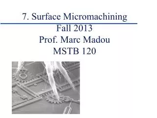
This fall 2013 course by Prof. Marc Madou covers the basics of microfabrication, focusing on single crystal growth methods like Czochralski and Float Zone. Topics include Si lattice structure, Miller Indices, isotropic and anisotropic etching, and Si crystal orientation. The course explores the diamond lattice structure of materials like silicon and germanium, along with the concept of Miller Indices for crystal planes in lattices. Wafer flats, wafer orientation, and the history of micromachining techniques are also discussed. This detailed study of bulk micromachining provides insights into semiconductor device fabrication processes and essential crystallographic principles.

E N D
6. Wet Bulk MicromachiningFundamentals of MicrofabricationFall 2013Prof. Marc MadouMSTB 120
Table of Content • Single crystal growth • Si lattice structure • Miller Indices • Wafer flats • Isotropic and anisotropic etching • Example
Bulk Micromachining • Semiconductor grade devices cannot be fabricated directly from Poly-Si, first we need to produce single crystal ingots, also the mechanical properties of single crystal Si are superior • Major methods are: Czochralski and Float Zone method Si crystal growth- Czochralsky method http://www.egg.or.jp/MSIL/english/msilhist0-e.html from Mitsubishi Materials Silicon Corporation
Bulk Micromachining Si crystal growth: float-zone crystal growth http://www.egg.or.jp/MSIL/english/msilhist0-e.html from Mitsubishi Materials Silicon Corporation
The Si diamond lattice is composed of two interpenetrating fcc lattices, one displaced 1/4 of a lattice constant from the other. Each site is tetrahedrally coordinated with four other sites in the other sublattice. When the two sublattices are of different atoms, then the diamond lattice becomes the zincblende or sphalerite lattice. Examples of materials with the diamond crystal structure are diamond, silicon and germanium. Bulk Micromachining
Si crystal orientation Bulk Micromachining Each site is tetrahedrally coordinated with four other sites in the other sublattice More atoms per cm 2 (oxidizes faster than 100) but etches much slower Equivalent planes i.e. families {} http://www.novagate.com/~ahines/rocks/vir_cris.htm
Bulk Micromachining Miller indices • Miller Indices are a symbolic vector representation for the orientation of an atomic plane in a crystal lattice and are defined as the reciprocals of the fractional intercepts which the plane makes with the crystallographic axes • To determine Miller indices of a plane take the following steps: 1. Determine the intercepts of the plane along each of the three crystallographic directions 2. Take the reciprocals of the intercepts 3. If fractions result, multiply each by the denominator of the smallest fraction
Miller indices Bulk Micromachining • The first thing that must be ascertained is the fractional intercepts that the plane/face makes with the crystallographic axes, in other words, how far along the unit cell lengths does the plane intersect the axis? in the figure, the plane intercepts each axis at exact one unit length (1) • Step two involves taking the reciprocal of the fractional intercept of each unit length for each axis, in the figure above, the values are all 1/1. (2) • Finally the fractions are cleared (i.e., make 1 as the common denominator) (3) • These integer numbers are then parenthetically enclosed and designate that specific crystallographic plane within the lattice. Since the unit cell repeats in space, the notation actually represents a family of planes, all with the same orientation. In the figure above, the Miller indices for the plane are (111) Miller Indices http://www.gly.uga.edu/schroeder/ gly630/millerindices.html
Bulk Micromachining • This figure shows a 4 inch 100 plane crystal Silicon wafer, typically between 250-600 microns thick • The current fab standards are up to 12 inch wafers • For CMOS work (100) and (111) (for bipolar) wafers are most important but in MEMS other orientations are used as well (especially (110) • Wafer flats indicate orientation (primary) and conductivity type (secondary)
Bulk Micromachining The primary flat on (100) and (111) wafers marks the <110> direction (100) (111) Purpose and Function Orientation for automatic equipment Indicate type and orientation of crystal Primary Flat = The flat of longest length located in the circumference of the wafer. The primary flat has a specified crystal orientation relative to the wafer surface; major flat. Secondary Flat = Indicates the crystal orientation and doping of the wafer. The location of this flat varies. P type <111> No secondary Flat P type <100> 90°±5° Clockwise from Primary Flat N type <111> 45°±5° Clockwise from Primary Flat N type <100> 180°±5° Clockwise from Primary Flat m Prima
Chemical milling: using a maskant and a scribe followed by acid to etch the scribed area Chemical milling (15 th century decorating armor) Chemical milling by the 1960’s especially used by the aerospace industry Photosenstive masks instead of scribing by hand (Niepce in 1822) Printed circuit board (WW II) Isotropic etching of Si (mid 1950’s) IC’s (1961) First Si micromechanical element (1961-1962) Anisotropic etching of Si (mid 1960’s) Bulk Micromachining
Flat [110] (111) L (110) a Anisotropic etching: [100] Si Bulk Micromachining • Proper alignment leads to {111} sidewalls, (100) bottom, <110> directed edges and <211> directed ribs • Consider the unit cube and the off-normal angle of the intersection of a (111) sidewall and a (110) cross-secting plane =arctan = 35.26°or 54.74° for the complementary angle
Anisotropic etching: [100] Si Bulk Micromachining • The width of the square bottom cavity wo is determined by the etch depth z, the mask opening and the angle we just calculated • To create a dense array of vias the Si wafer must be thinned
There are {100} planes perpendicular to the wafer surface (at a 45° angle with the wafer flat i.e.the {110} direction) Anisotropic etching: [100] Si Bulk Micromachining (100) planes Flat [110]
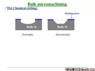
Bulk Micromachining Isotropic etching (HF:Nitric Acid: Acetic Acid) Anisotropic etching (KOH) (110) (100)
Isotropic etchants etch in all crystallographic directions at the same rate: Usually acidic (HNA i.e. HF, HNO3 and CH3COOH) Room temperature or slightly above (< 50 °C) Diffusion limited Etching is very fast (e.g. up to 50 µm min-1) Undercuts mask Masking very difficult e.g Au/Cr or LPCVD Si3N4 is good, but SiO2 is used because it is so simple Bulk Micromachining Stirring No stirring
Anisotropic etchants etch at different rates depending on the orientation of the exposed crystal plane: Usually alkaline (pH> 12 e.g. KOH) Higher temperatures (> 50 °C e.g. 85 to 115 °C) Reaction rate limited Slower e.g 1 µm/min (for <100> direction) Does not undercut the mask Not very agitation sensitive Masking very difficult e.g. LPCVD Si3N4 Bulk Micromachining
A typical bulk micromachining example: to make an array of electrochemical sensors in a catheter (e.g. to measure pH, O2 and CO2 in blood) The etch stop in this case is a sacrificial oxide layer Yet smaller structurs could be used to experiment in picoliter microvials (e.g. to investigate a single biological cell)-go visit http://pubs.acs.org/hotartcl/chemtech/98/feb/exper.html Bulk Micromachining Example: electrochemical sensor array
As in most cases the packaging is the more difficult and more expensive part of the sensor fabrication Bulk Micromachining Example: electrochemical sensor array
Example: electrochemical sensor array Bulk Micromachining • The sensor array is mounted in a catheter (750 µm diameter) • Biocompatible materials is still a very big issue • CAD of the sensor array