Download
1 / 21
230 likes | 382 Views
EE 5340 Semiconductor Device Theory Lecture 9 – Fall 2010. Professor Ronald L. Carter ronc@uta.edu http://www.uta.edu/ronc. Test 1 – W 29Sep10. 11 AM Room 108 Nedderman Hall Covering Lectures 1 through 10 Open book - 1 legal text or ref., only. You may write notes in your book.

E N D
EE 5340Semiconductor Device TheoryLecture 9 – Fall 2010 Professor Ronald L. Carter ronc@uta.edu http://www.uta.edu/ronc
Test 1 – W 29Sep10 • 11 AM Room 108 Nedderman Hall • Covering Lectures 1 through 10 • Open book - 1 legal text or ref., only. • You may write notes in your book. • Calculator allowed • A cover sheet will be included with full instructions. For examples see http://www.uta.edu/ronc/5340/tests/.
Poisson’s Equation • The electric field at (x,y,z) is related to the charge density r=q(Nd-Na-p-n) by the Poisson Equation:
Poisson’s Equation • n = no + dn, and p = po + dp, in non-equil • For n-type material, N = (Nd - Na) > 0, no = N, and (Nd-Na+p-n)=-dn +dp +ni2/N • For p-type material, N = (Nd - Na) < 0, po = -N, and (Nd-Na+p-n) = dp-dn-ni2/N • So neglecting ni2/N
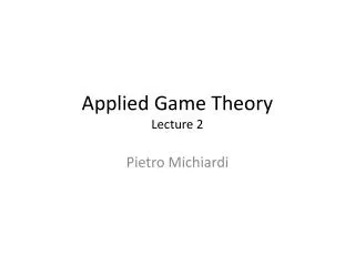
No disc in Eo Ex=0 in metal ==> Eoflat fBn=fm- cs = elec mtl to s/c barr fbi=fBn-fn= fm-fs elect s/c to mtl barr Ideal metal to n-typebarrier diode (fm>fs,Va=0) n-type s/c metal 0 xn xnc Eo qcs qfm qfbi qfs,n qfBn Ec EFm EFn EFi Depl reg Ev qf’n
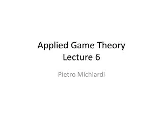
DepletionApproximation • For 0 < x < xn, assume n << no = Nd, sor = q(Nd-Na+p-n) = qNd • For xn < x < xnc, assume n = no = Nd, sor = q(Nd-Na+p-n) = 0 • For x = 0-, there is a pulse of charge balancing the qNdxn in 0 < x < xn
Ideal n-type Schottky depletion width (Va=0) Ex r xn qNd x Q’d = qNdxn x xn -Em d (Sheet of negative charge on metal)= -Q’d
n Nd 0 xn x Debye length • The DA assumes n changes from Nd to 0 discontinuously at xn. • In the region of xn, Poisson’s eq is E = r/e --> dEx/dx = q(Nd - n), and since Ex = -df/dx, we have -d2f/dx2 = q(Nd - n)/e to be solved
Debye length (cont) • Since the level EFi is a reference for equil, we set f = Vt ln(n/ni) • In the region of xn, n = ni exp(f/Vt), so d2f/dx2 = -q(Nd - ni ef/Vt), let f = fo + f’, where fo = Vt ln(Nd/ni) so Nd - ni ef/Vt = Nd[1 - ef/Vt-fo/Vt], for f - fo = f’ << fo, the DE becomes d2f’/dx2 = (q2Nd/ekT)f’, f’ << fo
Debye length (cont) • So f’= f’(xn) exp[+(x-xn)/LD]+con. and n = Nd ef’/Vt, x ~ xn, where LD is the “Debye length”
Debye length (cont) • LD estimates the transition length of a step-junction DR. Thus, • For Va = 0, i ~ 1V, Vt ~ 25 mV d< 11% DA assumption OK
Effect of V 0 • Define an external voltage source, Va, with the +term at the metal contact and the -term at the n-type contact • For Va > 0, the Va induced field tends to oppose Ex caused by the DR • For Va < 0, the Va induced field tends to aid Ex due to DR • Will consider Va < 0 now
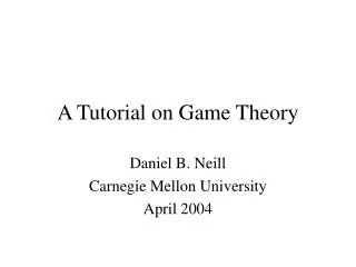
qVa = Efn - Efm Barrier for electrons from sc to m reduced toq(fbi-Va) qfBn the same DR decr Ideal metal to n-typeSchottky (Va > 0) metal n-type s/c Eo qcs qfm q(fi-Va) qfs,n qfBn Ec EFm EFn EFi Ev Depl reg qf’n
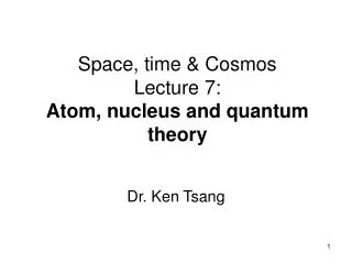
Schottky diodecapacitance r qNd Q’d = qNdxn dQ’ x -Q-dQ xn Ex xn x -Em
Schottky Capacitance(continued) • The junction has +Q’n=qNdxn (exposed donors), and Q’n = - Q’metal (Coul/cm2), forming a parallel sheet charge capacitor.
Schottky Capacitance(continued) • This Q ~ (i-Va)1/2 is clearly non-linear, and Q is not zero at Va = 0. • Redefining the capacitance,
Schottky Capacitance(continued) • So this definition of the capacitance gives a parallel plate capacitor with charges dQ’n and dQ’p(=-dQ’n), separated by, L (=xn), with an area A and the capacitance is then the ideal parallel plate capacitance. • Still non-linear and Q is not zero at Va=0.
Schottky Capacitance(continued) • The C-V relationship simplifies to
Schottky Capacitance(continued) • If one plots [Cj]-2vs. Va Slope = -[(Cj0)2Vbi]-1 vertical axis intercept = [Cj0]-2 horizontal axis intercept = fi Cj-2 Cj0-2 Va fi
References 1Device Electronics for Integrated Circuits, 2 ed., by Muller and Kamins, Wiley, New York, 1986. See Semiconductor Device Fundamentals, by Pierret, Addison-Wesley, 1996, for another treatment of the m model. 2Physics of Semiconductor Devices, by S. M. Sze, Wiley, New York, 1981. 3Semiconductor Physics & Devices, 2nd ed., by Neamen, Irwin, Chicago, 1997.