Download
1 / 28
450 likes | 1.02k Views
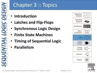
Sequential Logic Latches & Flip-flops. Introduction Memory Elements Pulse-Triggered Latch S-R Latch Gated S-R Latch Gated D Latch Edge-Triggered Flip-flops S-R Flip-flop D Flip-flop J-K Flip-flop T Flip-flop Asynchronous Inputs. Combinational outputs. Memory outputs.

E N D
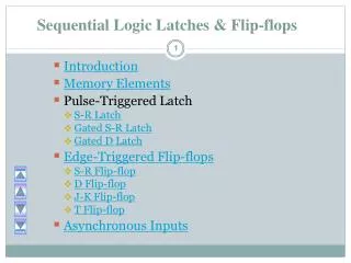
Sequential Logic Latches & Flip-flops • Introduction • Memory Elements • Pulse-Triggered Latch • S-R Latch • Gated S-R Latch • Gated D Latch • Edge-Triggered Flip-flops • S-R Flip-flop • D Flip-flop • J-K Flip-flop • T Flip-flop • Asynchronous Inputs
Combinational outputs Memory outputs Combinational logic Memory elements External inputs Introduction • A sequential circuit consists of a feedback path, and employs some memory elements. Sequential circuit = Combinational logic + Memory Elements
Introduction • There are two types of sequential circuits: • synchronous: outputs change only at specific time • asynchronous: outputs change at any time • Multivibrator: a class of sequential circuits. They can be: • bistable (2 stable states) • monostable or one-shot (1 stable state) • astable (no stable state) • Bistable logic devices: latches and flip-flops. • Latches and flip-flops differ in the method used for changing their state.
Q Memory element command stored value Memory Elements • Memory element: a device which can remember value indefinitely, or change value on command from its inputs. • Characteristic table: Q(t): current state Q(t+1) or Q+: next state
Q Memory element command stored value clock Positive pulses Positive edges Negative edges Memory Elements • Memory element with clock. Flip-flops are memory elements that change state on clock signals. • Clock is usually a square wave.
Memory Elements • Two types of triggering/activation: • pulse-triggered • edge-triggered • Pulse-triggered • latches • ON = 1, OFF = 0 • Edge-triggered • flip-flops • positive edge-triggered (ON = from 0 to 1; OFF = other time) • negative edge-triggered (ON = from 1 to 0; OFF = other time)
S-R Latch • Complementary outputs: Q and Q'. • When Q is HIGH, the latch is in SET state. • When Q is LOW, the latch is in RESET state. • For active-HIGH input S-R latch(also known as NOR gate latch), R=HIGH (and S=LOW) a RESET state S=HIGH (and R=LOW) a SET state both inputs LOW a no change both inputs HIGH aQ and Q' both LOW (invalid)!
S-R Latch • For active-LOW input S'-R' latch(also known as NAND gate latch), R'=LOW (and S'=HIGH) a RESET state S'=LOW (and R'=HIGH) a SET state both inputs HIGH a no change both inputs LOW aQ and Q' both HIGH (invalid)! • Drawback of S-R latch: invalid condition exists and must be avoided.
S R Q Q' S R Q Q' S-R Latch • Characteristics table for active-high input S-R latch: • Characteristics table for active-low input S'-R' latch:
R 1 0 0 1 0 1 1 0 0 0 Q Q' 0 0 1 0 1 S 0 0 0 1 1 S' Q S' Q Q' R' Q' R' S-R Latch • Active-HIGH input S-R latch • Active-LOW input S’-R’ latch
S Q S EN R Q Q' EN Q' R Gated S-R Latch • S-R latch + enable input (EN) and 2 NAND gates gated S-R latch.
EN=1 Q(t+1) = S + R'.Q S.R = 0 Gated S-R Latch • Outputs change (if necessary) only when EN is HIGH. • Under what condition does the invalid state occur? • Characteristic table:
D Q D EN Q Q' EN Q' Gated D Latch • Make R input equal to S' gated D latch. • D latch eliminates the undesirable condition of invalid state in the S-R latch.
When EN=1, Q(t+1) = D Gated D Latch • When EN is HIGH, • D=HIGH latch is SET • D=LOW latch is RESET • Hence when EN is HIGH, Q ‘follows’ the D (data) input. • Characteristic table:
Latch Circuits: Not Suitable • Latch circuits are not suitable in synchronous logic circuits. • When the enable signal is active, the excitation inputs are gated directly to the output Q. Thus, any change in the excitation input immediately causes a change in the latch output. • The problem is solved by using a special timing control signal called a clock to restrict the times at which the states of the memory elements may change. • This leads us to the edge-triggered memory elements called flip-flops.
Clock signal Positive edges Negative edges Edge-Triggered Flip-flops • Flip-flops: synchronous bistable devices • Output changes state at a specified point on a triggering input called the clock. • Change state either at the positive edge (rising edge) or at the negative edge (falling edge) of the clock signal.
S C R J C K D C Q Q' Q Q' Q Q' S C R J C K D C Q Q' Q Q' Q Q' Edge-Triggered Flip-flops • S-R, D and J-K edge-triggered flip-flops. Note the “>” symbol at the clock input. Positive edge-triggered flip-flops Negative edge-triggered flip-flops
S-R Flip-flop • S-R flip-flop: on the triggering edge of the clock pulse, • S=HIGH (and R=LOW) a SET state • R=HIGH (and S=LOW) a RESET state • both inputs LOW a no change • both inputs HIGH a invalid • Characteristic table of positive edge-triggered S-R flip-flop: X = irrelevant (“don’t care”) = clock transition LOW to HIGH
S-R Flip-flop • It comprises 3 parts: • a basic NAND latch • a pulse-steering circuit • a pulse transition detector (or edge detector) circuit • The pulse transition detector detects a rising (or falling) edge and produces a very short-duration spike.
S Q Pulse transition detector CLK Q' R CLK' CLK' CLK CLK CLK* CLK* CLK CLK CLK' CLK' CLK* CLK* Positive-going transition (rising edge) Negative-going transition (falling edge) S-R Flip-flop The pulse transition detector.
D S C R Q Q' CLK D Flip-flop • D flip-flop: single input D (data) • D=HIGH a SET state • D=LOW a RESET state • Q follows D at the clock edge. • Convert S-R flip-flop into a D flip-flop: add an inverter. = clock transition LOW to HIGH A positive edge-triggered D flip-flop formed with an S-R flip-flop.
Q1 = X* D CLK D CLK D CLK Q Q' Q Q' Q Q' X Combinational logic circuit Y Q2 = Y* Z Q3 = Z* Transfer * After occurrence of negative-going transition D Flip-flop • Application: Parallel data transfer. To transfer logic-circuit outputs X, Y, Z to flip-flops Q1, Q2 and Q3 for storage.
J-K Flip-flop • J-K flip-flop: Q and Q' are fed back to the pulse-steering NAND gates. • No invalid state. • Include a toggle state. • J=HIGH (and K=LOW) a SET state • K=HIGH (and J=LOW) a RESET state • both inputs LOW a no change • both inputs HIGH a toggle
J Q Pulse transition detector CLK Q' K J-K Flip-flop • J-K flip-flop. • Characteristic table. Q(t+1) = J.Q' + K'.Q
T T J C K Q Q' Q Pulse transition detector CLK CLK Q' T Flip-flop • T flip-flop: single-input version of the J-K flip flop, formed by tying both inputs together. • Characteristic table. Q(t+1) = T.Q' + T'.Q
High High High QA QB J C K J C K J C K Q CLK CLK CLK CLK QA Q QB Divide clock frequency by 2. Divide clock frequency by 4. T Flip-flop • Application: Frequency division. • Application: Counter (to be covered in Lecture 13.)
Asynchronous Inputs • S-R, D and J-K inputs are synchronous inputs, as data on these inputs are transferred to the flip-flop’s output only on the triggered edge of the clock pulse. • Asynchronous inputs affect the state of the flip-flop independent of the clock; example: preset (PRE) and clear (CLR) [or direct set (SD) and direct reset (RD)] • When PRE=HIGH, Q is immediately set to HIGH. • When CLR=HIGH, Q is immediately cleared to LOW. • Flip-flop in normal operation mode when both PRE and CLR are LOW.
PRE PRE J C K Q Q' J CLR CLR Q Pulse transition detector CLK Q' K CLK PRE CLR Q J = K = HIGH Preset Toggle Clear Asynchronous Inputs • A J-K flip-flop with active-LOW preset and clear inputs.