
PXD Summary
E N D
Presentation Transcript
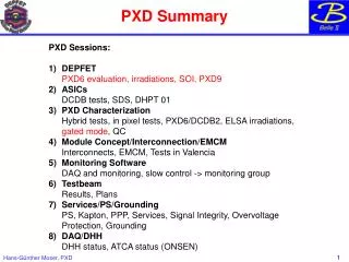
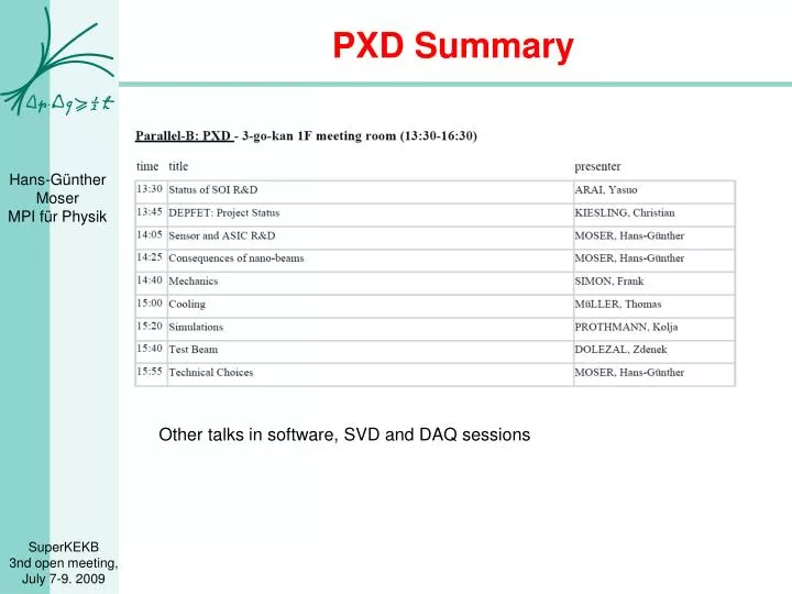
PXD Summary Other talks in software, SVD and DAQ sessions
SOI Detectors Yasuo Arai *1st MPW: submission on 7th Aug. 2009 *2nd MPW: submission on end. Oct. 2010 *3rdMPW: submission on beg. Jan. 2010 We have received several contacts from foreign labs ; India, UK, Spain, USA, Poland ... This possibility has been announced by the facilitation group for monolithic and vertically integrated pixel detectors (Marcel Demarteau, Junji Haba, Hans-Günther Moser and Valerio Re). Thus collaborations for R&D should be initiated pushing progress for such detectors
Without BPW With BPW B (~1E12 cm-2) Vback Up BPW SOI R&D at KEK Laser test of SBPIX1 48x48 pixels of 50x50µm² New: buried p-well to reduce back gate effect:
DEPFET: Ringberg Workshop http://indico.mppmu.mpg.de/indico/conferenceDisplay.py?confId=466
DEPFET-Collab. @ Belle-II Original Collaboration: DEPFET pixel detector @ ILC (since 2002) now: Unite efforts to deliver a REAL PXD by 2013 for Belle-II University of Barcelona, Spain University Ramon Llull, Barcelona, Spain Bonn University, Germany Heidelberg University, Germany Giessen University, Germany Göttingen University, Germany Karlsruhe University, Germany IFJ PAN, Krakow, Poland MPI Munich, Germany Charles University, Prague, Czech Republic IGFAE, Santiago de Compostela University, Spain IFIC, CSIC-UVEG, Valencia, Spain DEPFET@Belle-II New management: IB- Board Project Leader C. Kiesling Technical Coord. H.-G. Moser „Integration Coord.“ (Liaison @ KEK) with important help from Hawaii, KEK, Vienna
Sensor Production Status Status at 2nd Belle II meeting (March): SOI wafer bonding at Tracit, France 30 SOI wafers received, processing in our own lab has started Presently: cleaning, oxygenation, alignment mask, first implantation: next week. Processed are 6 wafers + dummies
Wafer layout Small test matrices with various pixel sizes; 50 µm x 50 µm .. 50 µm x 175 µm Technology variations (gate length L) 4 ½ module large matrices with most likely pixel sizes 5cm: 50µm x 75µm 5cm: 50µm x 100µm 3.5cm 50µm x 50µm 3.5cm 50µm x 75µm Important for timing!
DEPFET Readout and Control ASICs DCD, Switcher: Heidelberg DHP: Bonn, Barcelona
DCD Tests Manuel Koch, Bonn • Works almost at design frequency (540 MHz: 88ns line rate) • (works still at nominal 600 MHz, but with higher noise) • Noise level: 90nA with 450 pA/e: 200 e ENC (S/N = 20:1) • Some bugs discovered, improved version will be submitted • Push DEPFET gain (600 pA/e ?)
Summary: ASICs • - DCD prototype chip has been tested with test signals that correspond to DEPFET currents and irradiated up to 7 Mrad. • The chip works fine and has high enough conversion speed. • Operation with matrices still to be tested – we do not expect problems. • Only „fine tuning“ of the design for the super KEKB operation is necessary. • - Switcher prototype with LV transistors has been tested and irradiated up to 22 MRad. • The chip works fine and has adequate speed for Belle II operation. • - Another prototype with HV transistors has been designed and tested. • - The irradiation of the chip still has to be done but the basic and most critical part (high-voltage NMOS) has been irradiated up to 600 KRad and no damage has been observed. • - DHP chip will be designed using digital design tools in intrinsically radiation hard 90 nm technology. • - Choice between 4 different bumping technologies – advantages and disadvantages still to be evaluated • Planned submissions: • Switcher: October 09 • DCD: September 09 • DHP: October 09
Consequences of nano beam Less background? Always welcome, but to be confirmed Smaller beam pipe: 1.5cm -> 1.0cm 1cm beam pipe allows: 1st layer closer to the beam => better resolution Smaller modules with smaller pitch (in z) => better resolution Smaller modules: better use of wafer size: higher yield less wafers needed? more space for electronics and cooling More freedom to choose layer spacing optimize resolution improve mechanical layout (symmetric arrangement?) (more room for cooling/services?) Major work needed to find optimum! Need final geometry of IR (and beam pipe outer radius) soon!
Mechanics Frank Simon:
Mechanics New simpler concept for support More space for services and air flow Integrated cooling channels Sliding module mount (termal expansion)
DCDs always active: The hottest points • 2 Switchers active • 2 pixel stripes active We need to cool down the DCD Cooling Thomas Müller (work done in Karlsruhe and Valencia) Power: ca 7W per module half 6 W: ASIC on end 1 W: sensor area Total ~ 300 W Needs both liquid and air cooling Highly thermally conductive materials needed to get heat out of module Under study: TPG (thermally pyrolythic graphite) CVD diamond Work started, tooling to be set up (simulation, mock ups)
Simulations Kolja Prothman (work done in Munich and Prague) Important tool for parameter optimisation (pitch, layer radius, pixel arrangments Simulated is PXD with active and passive material SVD and CDC Some examples
Simulations Variable pitch and bricking not usefull Smaller pitch with longer readout time improves IP(z) resolution considerably Performance better than Belle SVD Most work done assuming 1.5 cm IR Work on nano beam geometry started => should be even better
Test Beam Zdenek Dolezal for test beam group • 6 plane telescope (incl. DUT) • IL-like pixels (24 µm pitch) • Thick silicon (450 µm) • ‘old’ readout & control ASICs • Learn a lot about DEPFET operation • Tuning of operation parameters • X-check and tuning of simulation Next test beam end of July Belle II type test beam in 2010
Technical choices Important: need to fix geometry: radius, module length, thickness latest possibility: September 2010 (prepare SOI material) Details on pitch can wait till March 2011 Driven by sensor production schedule However, engineering of support and cooling including prototyping should start soon: need to fix parameters this year!
Parameter choices Options like bricked pixels of variable pitch were abandoned in Ringberg (However: variable pitch may come back due to 1cm beam pipe?) Major decision to take: 10µs or 20µs frame readout time? longer readout time allows smaller pixel, better resolution slightly higher (but still tolerable) occupancy higher readout bandwidth needed 20µs favoured in Ringberg have to study again for nano-beam Some ideas to improve DCD readout speed (no DCS): not baseline Important: Redundancy: Choose parameters (speed, pitch etc) not at the limit of the technology! Give some headroom in case some specs are not reached: e.g. DT(line readout) x N(lines) < 10µs (e.g. use abort gap as ‘buffer’)