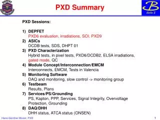
PXD Summary
PXD Summary. PXD Sessions: DEPFET PXD6 evaluation, irradiations, SOI, PXD9 2) ASICs DCDB tests, SDS, DHPT 01 3) PXD Characterization Hybrid tests, in pixel tests, PXD6/DCDB2, ELSA irradiations, gated mode , QC 4) Module Concept/Interconnection/EMCM

PXD Summary
E N D
Presentation Transcript
PXD Summary PXD Sessions: DEPFET PXD6 evaluation, irradiations, SOI, PXD9 2) ASICs DCDB tests, SDS, DHPT 01 3) PXD Characterization Hybrid tests, in pixel tests, PXD6/DCDB2, ELSA irradiations, gated mode, QC 4) Module Concept/Interconnection/EMCM Interconnects, EMCM, Tests in Valencia 5) Monitoring Software DAQ and monitoring, slow control -> monitoring group 6) Testbeam Results, Plans 7) Services/PS/Grounding PS, Kapton, PPP, Services, Signal Integrity, Overvoltage Protection, Grounding 8) DAQ/DHH DHH status, ATCA status (ONSEN)
PXD6 tests Measuremtents of full size matrices started
Irradiations PXD6 has a wet oxide instead the dry oxide of previous versions Wet oxide turns out to be more radiation hard than dry one => We can use nitride with a comfortable thickness !
SOI Processing of PXD9 scheduled to start February 2012 Had to stop processing Need to repair wafers or procure new ones
SOI: next steps • Repair wafers (cover edge with poly, re-polish, inspect) restart in March • ICEMOS will try a new edge treatment • (etching instead of grinding) restart in May • 3) Wafers from Shin Etsu • edge quality of standard wafers ok • bonding ok (but not with the edge quality required) • need more R&D restart in August • Need to re-schedule • Plan with prototype run & main production: already late (finish PXD end 2015!) • PXD9 will become main production • Even with 6 months delay (Shin Etsu): PXD ready in time (August 2015) • Backup production still possible if yield low (but with a delay) -> plan B
Injection Noise: Gated DEPFET Injected bunches are noisy and spoil data Can we gate the DEPFET during the passage of a noisy bunch? ~ 20% loss of data (with some uncertainty about actual damping time)
Gated operation Potential difference controlled by external gate
Simulation Measurements will be done by Felix Müller. stay tuned! Note: even a slight penalty in performance would outweigh a 20% loss of data!
Caveats Potential problems: large currents for global clear: 30 mA more power: 360mW/module need caps (2 x 200 nF); where? modifications of switcher, DHP needed complicated readout cycle
Dynamic Range • We need a certain dynamic range to see a signal of up to 2.5 MIPs (? tbc) with 128 bit resolution • On top of • DEPFET/DCD pedestal spread • Common mode fluctuations (per input line) • Variations due to radiation damage (threshold voltage shift) • Basics: • Max. baseline compensation of DCD-B2: 200µA (common for each DCD) • Input current compensation: up to 0/8/16/24 µA (2 bit DAC) • Option in DCD-B2: input common mode compensation up to 200µA (300 ? tbc, not yet tested)
DEPFET current range geometry Threshold voltage: depends on irradiation Gate voltage: adjustable Inhomogeneous threshold voltage shift leads to a large pedestal dispersion! And to a dispersion of the DEPFET gain, too!
Data versus Model Good agreement till ~ 125 µA (thendeviations fromthe simple model are expected)
Pedestal Spread Rather large pedestal spread in Hybrid 4.1.04 100 ADC counts => 10µA ~ 0.3 volt shift Some gradient along and across matrix But, this is a small matrix! Perhaps, this is a somehow sick matrix Need more statistics and systematic investigations
Threshold voltage difference Thin wet oxide (like in PXD6) Factor 3 difference In fact: module divided in three sections Facto3 3 across 1.1 cm! Anyway: Max DV < 1.5V A. Ritter
Pedestal Compensation Raw pedestals After baseline comp. After DAC subtraction. DAC 11 24 µA 8 µA DAC 10 16 µA Min signal range: 8µA 128 steps Max pedestal spread: 32µA DAC 01 8 µA ADC: 16µA 256 steps DAC 00 0 µA Input CM compensation <200µA (in steps of <2µA – 7bits?) Option in DCD-B2: input CM compensation <200µA ADC step 16µA/256 = 62.5nA
Max allowed pedestal spread of 32µA • Residual dynamic range for signal: 8 µA • MIP ~ 2.7 µA (gq 0.45nA/e): 3 MIPs! • but: common mode! • Input CM compensation should help • may be affected by disconnected or noisy channels: • One noisy channel with 100µA offset would give 0.4µA offset: ok • 6/256 channels disconnected: CM wrong by 2%: 2µA for 100µA offset: probably still ok • Real hit: 2.7µA/250 ~ 0.01µA, negligible • Nevertheless: this is a 2nd order effect and will be exactly corrected by the DHP • We just have to make sure that the residual CM does not saturate the dynamic range
Range if we have DAQ only Lower limit of Id: minimum acceptable qg => minimum signal/noise Assume: S/N > 20:1 Noise 100 nA Signal: 2µA for 6000 electrons => gq(min) = 0.33 nA/e For L=5µm W=20µA we need Id(min)=34µA @ 1.2V Upper limit of Id (DAC range) : Id(max) = Id(min) + 32µA = 66µA The max voltage shift which keeps Id between 34µA and 66 µA is ~ 0.4 V gq varies between 0.33 nA/e to 0.44 nA/e
with input CM compensation Lower limit of Id: minimum acceptable qg => minimum signal/noise Assume: S/N > 20:1 Noise 100 nA Signal: 2µA for 6000 electrons => gq(min) = 0.33 For L=5µm W=20µA we need Id(min)=34µA @ 1.2V Upper limit of Id: can compensate shifts up to full DCD range (200µA): Id(max) = 200µA – signal range (8µA) = 192µA The max voltage shift which keeps Id between 34µA and 192 µA is ~ 1.6 V gq varies beween 0.33 nA/e to 0.76 nA/e (a MIP is 4.5µA!) This would be ok, given the expectations! (and, we still have the segmentation!)
Conclusions Main worry: availability of SOI material! Project already delayed! Rely on improvements at ICEMOS (in work) and/or Shin Etsu Otherwise, things look pretty good Noteworthy: gated operation to suppress injection noise seems possible However: system aspects (power, current) Need to understand operation parameters: pedestal spread dynamic range max. compensable threshold voltage shift! Need to change attitude: from proof of principle => limits of operation We need to implement “imperfections” in MC Need guidance what performance parameters are critical!