IC Logic Families
440 likes | 746 Views
IC Logic Families. Wen-Hung Liao, Ph.D. Digital IC Terminology. Voltage Parameters: V IH (min): high-level input voltage, the minimum voltage level required for a logic 1 at an input . V IL (max): low-level input voltage V OH (min): high-level output voltage

IC Logic Families
E N D
Presentation Transcript
IC Logic Families Wen-Hung Liao, Ph.D
Digital IC Terminology • Voltage Parameters: • VIH(min): high-level input voltage, the minimum voltage level required for a logic 1 at an input. • VIL(max): low-level input voltage • VOH(min): high-level output voltage • VOL(max): low-level output voltage
Current Parameters • IIH(min): high-level input current, the current that flows into an input when a specified high-level voltage is applied to that input. • IIL(max): low-level input current • IOH(min): high-level output current • IOL(max): low-level output current
Fan-Out • The maximum number of standard logic inputs that an output can drive reliably. • Also known as the loading factor. • Related to the current parameters (both in high and low states.)
Propagation Delays • tpLH: delay time in going from logical 0 to logical 1 state (LOW to HIGH) • tpHL: delay time in going from logical 1 to logical 0 state (HIGH to LOW) • Measured at 50% points.
Power Requirements • Every IC needs a certain amount of electrical power to operate. • Vcc (TTL) • VDD(MOS) • Power dissipation determined by Icc and Vcc. • Average Icc(avg)= (ICCH + ICCL)/2 • PD(avg) = Icc(avg) x Vcc
Speed-Power Product • Desirable properties: • Short propagation delays (high speed) • Low power dissipation • Speed-power product measures the combined effect.
Noise Immunity • What happens if noise causes the input voltage to drop below VIH(min) or rise above VIL(max)? • The noise immunity of a logic circuit refers to the circuit’s ability to tolerate noise without causing spurious changes in the output voltage. • Noise margin: Figure 8-4. • VNH=VOH(min)-VIH(min) • VNL=VIL(max)-VOL(max) • Example 8-1.
Invalid Voltage Levels • For proper operation the input voltage levels to a logic must be kept outside the indeterminate range. • Lower than VIL(max) and higher than VIH(min).
IC Packages • DIP • J-Lead • Gull-wing • Table 8-2 for a complete list.
The TTL Logic Family • Transistor-transistor logic • Figure 8-7: NAND gate. • Circuit operation: LOW state, current-sinking • Circuit operation: HIGH state, current-sourcing.
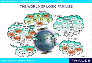
Standard TTL Series Characteristics • TI introduced first line of standard TTL: 54/74 series (1964) • Manufacturers’ data sheets (Figure 8-11) • Supply voltage and temperature range • Voltage levels • Maximum voltage ratings • Power dissipation • Propagation delays • Fan-out • Example 8-2
Improved TTL Series • 74 Series • Schottky TTL, 74S Series: higher speed • Low-Power Schottky TTL, 74LS series • Advanced Schottky TTL, 74AS Series • Advanced Low-Power Schottky TTL, 74ALS Series • 74F-Fast TTL
Examples • Example 8-3: Noise margin of 74 and 74LS • Example 8-4: TTL series with max number of fan-out
TTL Loading and Fan-Out • Figure 8-13: currents when a TTL output is driving several inputs. • TTL output has a limit, IOL(max), on how much current it can sink in the LOW state. • It also has a limit, IOH(max), on how much current it can source in the HIGH state.
Determining the fan-out • Same IC family. • Find fan-out (LOW):IOL(max)/IIL(max) • Find fan-out (HIGH):IOH(max)/IIH(max) • Fan-out: smaller of the above • Example 8-6: Fan-out of 74AS20 NAND gates
Determining the fan-out • Different IC families • Step 1: add up the IIH for all inputs connected to an output. The sum must be less than the output’s IOH specification. • Step 2: add up the IIL for all inputs connected to an output. The sum must be less than the output’s IOL specification. • Examples 8-7 to 8-9.
Other TTL Characteristics • Unconnected inputs (floating): acts like a logic 1. • Unused inputs: three different ways to handle. • Tie-together inputs: common input generally represent a load that is the sum of the load current rating of each individual input. Exception: for AND and NAND gates, the LOW state input load will be the same as a single input no matter how many inputs are tied together. • Example 8-10.
Other TTL Characteristics (cont’d) • Current transients (Figure 8-18) • Connecting TTL outputs together • Totem-pole outputs should no be tied together
MOS Digital ICs • MOS: metal-oxide-semiconductor • MOSFET: MOS field-effect transistors. • The Good: • Simple • Inexpensive to fabricate • Small • Consumes little power • The bad: • Static-electricity damage. • Slower than TTL
The MOSFET • P-MOS: P-channel MOS • N-MOS: N-channel MOS, fastest • CMOS: complementary MOS, higher speed, lower power dissipation. • Figure 8-20: how N-channel MOSFET works: • VGS=0V OFF State, Roff= 1010 ohms • VGS=5V ON State,Ron=1000 ohms
N-MOS INVERTER Q1 Q2
CMOS • Uses both P- and N-channel MOSFETs in the same circuit to realize several advantages over the P-MOS and N-MOS families. • CMOS INVERTER (Figure 8-22) • CMOS NAND (Figure 8-23) • CMOS NOR (Figure 8-24)
CMOS Series Characteristics • Pin-compatible • Functionally equivalent • Electrically compatible • 4000/14000 Series • 74C, 74HC/HCT, 74AC/ACT, 74AHC, • BiCMOS (Bipolar + CMOS) • Table 8-10: low-voltage series characteristics • Table 8-11, comparison of ECL, CMOS and TTL Series
Low-Voltage Technology • 5V 3.3V • Reduces power dissipation • 74LVC, 74ALVC, 74LV, 74LVT
Other CMOS Issues • Conventional CMOS outputs should not be connected together. • Bilateral switch (Figure 8-43,44)
IC Interfacing • Connecting the output(s) of one circuit to the input(s) of another circuit that has different electrical characteristics. • Occurs often in complex digital systems, where designers utilize different logic families for different parts of system. • TTL driving CMOS • CMOS driving TTL
TTL driving CMOS • No problem with the current requirements (See Table 8-12) • VOH(min) of TTL is low compared to VIH(min) of some CMOS series (Table 8-9), use pull-up resistor to raise TTL output voltage (Figure 8-46) • TTL driving high-voltage CMOS (VDD of CMOS is greater than 5V) • Use 7407 buffer • Use voltage level-translator (such as 4504B)
CMOS driving TTL • HIGH state:Table 8-9 and 8-12 indicate no special consideration the HIGH state. • LOW state: depends on the series used.