Error Detecting Adder
Error Detecting Adder. Yugandhar Asmath Saikiran Vodela Pavan Polum Puneet Shrivastava Advisor: Dr. David W Parent 8 th May 2006. Agenda. Abstract Introduction Why Simple Theory Back Ground information (Literature Review) Summary of Results Project (Experimental) Details Results

Error Detecting Adder
E N D
Presentation Transcript
Error Detecting Adder Yugandhar Asmath Saikiran Vodela Pavan Polum Puneet Shrivastava Advisor: Dr. David W Parent 8th May 2006
Agenda • Abstract • Introduction • Why • Simple Theory • Back Ground information (Literature Review) • Summary of Results • Project (Experimental) Details • Results • Cost Analysis • Conclusions
Abstract • We designed an error detecting carry free adder based on the architecture proposed by Whitney J. Townsend, Jacob A. Abraham & Parag K. Lala. in ‘On-Line Error Detecting Constant Delay Adder’. • The data width was taken as four bits and the circuit was designed to operate at 200 MHz and had dimensions of 200.7x324.1 mm2 with a power consumption of 44.1 mW.
Introduction • Why the need for error tolerance? • What possibly could cause errors? • How can errors be detected? – Different error detecting codes • Hamming code • Gray code • m-out-of-n code • We have chosen to use the 1-of-3 code for error detection!
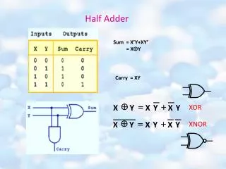
1-of-3 code in error detecting adder • We use constant delay arithmetic with decimal number representation. • As suggested in [1] and [2], we encode the binary inputs to the adder as • 0 is coded as 010 • 1 in any of the n-1 bits is coded as 001 • 1` (-1 in signed bit representation) in the MSB as 100 • The figure illustrates a two operand addition/error detection operation.
Project Summary • Inputs • Two 4-bit words as addend and augend. • A reset pin. • Clock • Outputs • A 4-bit sum. • One Carry bit. • Error indication pin. • Specs • Clock Frequency – 200MHz • Worst Propagation delay – 3.3ns. • Cell height 30 microns • Power consumption – 44.1 mW. • Area – 200 x 324 microns
Project Details • The 1-of-3 code is split into two 1-of-2 codes to simplify logic realization. • The encoder consists of a simple inverter. • Addition is carried out in two stages • The output of the 1st stage is called intermediate sum and carry. • The intermediate sum and carry are then summed up to get the final sum. • The final outputs in 1-of-3 code are then checked for errors using the checker circuit.
Longest Path Calculations Total t = 2.92 ns.
Simulations Propagation delay for post-extraction - 3.36ns Propagation delay for pre-extraction - 3.22ns
Cost Analysis • Time spent on each phase of the project • Designing the logic - 2 week • Verifying logic – 2 week • Verifying timing – 1 week • Layout – 2 weeks. • Post extraction verification – 2 days. • Total labour involved –200 hrs
Summary • Designed an error detecting carry free constant delay adder that works at 200MHz. • Extensively used the concepts learned as a part of EE166. • Used IC5.0 by Cadence systems to verify gate level logic and then lay out the logic in CMOS technology (AMI06 Process)
Lessons learnt • Start early, that’s the key to avoid last minute pressures. • Take full advantage of Dr.Parent’s expertise. • Work as a team, and plan well before you start. • Break the projects into smaller modules and proceed step by step. Don’t be ambitious.
References and Bibliography • On-Line Error Detecting Constant Delay Adder - Whitney J. Townsend, Jacob A. Abraham & Parag K. Lala. • On-Line Error Detection in a Carry-Free AdderWhitney J. Townsend and Mitchell A. Thornton Parag K. Lala. • Evolution of fault-tolerant and noise-robust digital designs - M. Hartmann and P.C. Haddow. • On the Design of Combinational Totally Self-checking 1-out-of-3 Code Checkers JIEN-CHUNG LO AND SUCHAI THANAWASTIEN. • A MOS Implementation of Totally Self-checking Checker for the 1-out-of-3 Code - D. L. TAO, PARAG K. LALA AND CARLOS R. P. HARTMAN • Acknowledgements • We thank Prof. Parent for his support and guidance which helped us in successfully completing the project. • We would thank the Cadence Design Systems to have generously let us use their tools in our Cadence lab. • We would also like to thank all our counterparts in this class who helped us in a way or the other.