1 / 20

Quasi-square-wave ZVS converters

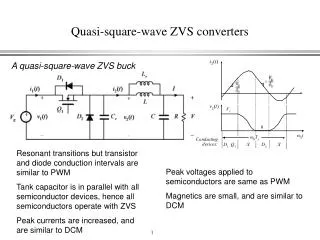
Quasi-square-wave ZVS converters. A quasi-square-wave ZVS buck. Resonant transitions but transistor and diode conduction intervals are similar to PWM Tank capacitor is in parallel with all semiconductor devices, hence all semiconductors operate with ZVS

beryl
Download Presentation

Quasi-square-wave ZVS converters

An Image/Link below is provided (as is) to download presentation Download Policy: Content on the Website is provided to you AS IS for your information and personal use and may not be sold / licensed / shared on other websites without getting consent from its author. Content is provided to you AS IS for your information and personal use only. Download presentation by click this link. While downloading, if for some reason you are not able to download a presentation, the publisher may have deleted the file from their server. During download, if you can't get a presentation, the file might be deleted by the publisher.

E N D

Presentation Transcript


  1. Quasi-square-wave ZVS converters A quasi-square-wave ZVS buck Resonant transitions but transistor and diode conduction intervals are similar to PWM Tank capacitor is in parallel with all semiconductor devices, hence all semiconductors operate with ZVS Peak currents are increased, and are similar to DCM Peak voltages applied to semiconductors are same as PWM Magnetics are small, and are similar to DCM

  2. Quasi-square-wave versions of other converters Flyback Boost Single transistor version of switch is restricted to 0.5 < µ < 1 So for boost, M > 2 For flyback, M > n Boost inductor and flyback transformer are very small, and are similar to DCM devices

  3. Interleaved quasi-square-wave buck converters as VRM

  4. Waveforms

  5. State plane

  6. Interval 1Q1 conduction

  7. Interval 2Resonant transition

  8. Interval 3Diode D2 conduction

  9. Interval 4Resonant Transition

  10. Interval 5D1 conduction

  11. Average switch input current

  12. Length of switching period

  13. Another approach: Find dc component of output current

  14. Average output current, p. 2

  15. Control input: transistor/diode conduction angle 

  16. A way to solve and plot the characteristics

  17. Solving, p 2

  18. Results: Switch conversion ratio µ vs. F

  19. Switch conversion ratio µ vs.  Course website contains Excel spreadsheet (with function macros) that evaluates the above equations and can plot the above characteristics.

More Related