Chapter 6 Function of Combination Logic
540 likes | 827 Views
Chapter 6 Function of Combination Logic. 6-1 Bisic Adders. 6-2 Parallel Binary Adders. 6-3 Comparators. 6-4 Decoders. 6-5 Encoders. 6-6 Code Converters. Chapter 6 Function of Combination Logic. 6-7 Multiplesers. 6-8 Demultiplesers. 6-9 Parity Generators.

Chapter 6 Function of Combination Logic
E N D
Presentation Transcript
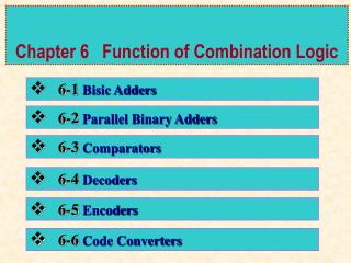
Chapter 6 Function of Combination Logic • 6-1 Bisic Adders • 6-2 Parallel Binary Adders • 6-3 Comparators • 6-4 Decoders • 6-5 Encoders • 6-6 Code Converters
Chapter 6 Function of Combination Logic • 6-7 Multiplesers • 6-8 Demultiplesers • 6-9 Parity Generators • 6-10 Troubleshooting • 6-11 Programmable Logic Devices • 6-12 Digital System Application
6-1 Bisic Adders Logic Circuit Give the express gradually predigest Truth Table Cive the logic function
6-1 Bisic Adders Half Adder
S= xy +xy C= xy 6-1 Bisic Adders
S=x⊕y C=xy
6-1 Bisic Adders Full Adder Truth Table
∑ CO CI
The full adder can be also implemented with two half adders and one OR gate.
F3 F2 F1 F0 CO CO ∑ ∑ CI CI CO CO ∑ ∑ CI CI B3 A3 B2 A2 B1 A1 B0 A0 6-2 Parallel Binary Adders Binary Adder C0 must be 0 4-Bit Adder
Only after the carry propagates and ripples through all stages will the output S4 and carry C4 settle to their final correct value. 6-2 Parallel Binary Adders Carry Propagation
Pi = Ai⊕ Bi Si = Pi⊕ Ci Ci+1 = Gi + Pi Ci Gi = Ai Bi 6-2 Parallel Binary Adders Carry lookahead
C0 = input carry C1 = G0+ P0 C0 C2 = G1+ P1 C1 = G1+ P1(G0+ P0 C0 ) = G1+ P1 G0+ P1 P0 C0 C3 = G2+ P2 C2 = G2+ P2 G1+ P2 P1 G0 + P2 P1 P0 C0 6-2 Parallel Binary Adders Carry lookahead Ci+1 = Gi + Pi Ci
F4⑽ F1⑷ F3⒀ F2⑴ CO4⑼ =1 =1 =1 =1 Y4 Y3 Y2 X4 X3 X2 X1 Y1 ≥1 ≥1 ≥1 ≥1 & & 1 & & & & & & & & & & & 1 & 1 1 1 & ≥1 & ≥1 & ≥1 & ≥1 1 A4⑿ A3⒁ B3⒂ A2⑶ B2⑵ A1⑸ B1⑹ CI1⑺ B4⑾
A0 0 3 COMP A1 P A2 A3 FP<Q FP=Q FP>Q P<Q P=Q P>Q A<B A=B A>B < = > B0 0 3 B1 Q B2 B3 6-3 Comparators Truth Table of 1 bit comparators
A0 0 3 COMP A1 P A2 A3 FP<Q FP=Q FP>Q P<Q P=Q P>Q A<B A=B A>B < = > B0 0 3 B1 Q B2 B3
(A > B) = A3 B3 + x3 A2 B2 + x3 x2 A1 B1 + x3 x2 x1 A0 B0 (A < B) = A3 B3 + x3 A2 B2 + x3 x2 A1 B1 + x3 x2 x1 A0 B0 6-3 Comparators if A ≠ B,
6-3 Comparators 4-Bit Magnitude Comparator
& Y0 1 1 1 1 1 ST & Y1 & Y2 A0 & A1 Y3 6-4 Decoders
Y0 Y2 Y1 ST Y3 BIN/OCT 0 1 2 3 1 2 A0 A1 EN 2-to-4-Line Decoder
Y3 Y1 Y2 Y0 ST ST Y1 Y3 Y0 Y2 3 2 1 0 3 2 1 0 BIN/OCT BIN/OCT Ⅰ Ⅱ 1 2 EN 1 2 EN 1 A0 A1 A2 Decoders with enable inputs can be connected together to form a larger decoder circuit.
Y3 Y0 Y2 Y1 STB STC Y7 Y6 Y4 Y5 BIN/OCT 0 1 2 3 1 2 4 A0 A1 A2 4 5 6 7 & STA EN 3-to-8-Line Decoder
A B C D VCC & & & & 1 1 1 1 9 8 7 6 5 4 3 2 1 0 1kW×9 6-5 Encoders An encoder is a digital circuit that performs the inverse operation of a decoder. 3-to-8-Line Decoder
YS(15) ≥1 ≥1 ≥1 ≥1 & & & & & & & & & & & & & 1 1 1 1 1 1 1 1 1 1 1 1 1 IN7(4) IN0(10) IN1(11) IN3(13) IN4(1) IN5(2) YEX(14) IN2(12) ST(5) Y0(9) Y1(7) Y2(6) IN6(3) CT54/74148
IN3 IN6 IN5 ST IN2 IN1 IN4 IN7 Y0 YEX Y2 Y1 IN0 HPRI/BIN 0/Z10 1/Z11 2/Z12 3/Z13 4/Z14 5/Z15 6/Z16 7/Z17 10 11 12 13 14 15 16 17 ≥1 YS 18 a V18 ENa 1a 2a 3a
ST 0 …… 7 8 …… 15 ST 0 1 2 3 4 5 6 7 EN 0 1 2 3 4 5 6 7 EN HPRI/BIN HPRI/BIN YS YS Y2 Y0 Y1 Y2 YEX Y0 Y0 YEX YEX Y1 Y2 Y1 Y3 & & & & Enlarge 8-3 line Encoder to 16-4 line Encoder
Output S1 through S3 have equal propagation delay times. 6-6 Code Converters 4-Bit Adder with Carry Lookahead
An-1 … A1 A0 D0 D0 D1 D1 D2 D2 MUX DMUX … … D2n-1 D2n-1 6-7 Multiplexers A multiplexer is a combinational circuit that selects binary information from one of many input lines and directs it to a single output line. Logic Diagram of 4-to-1-line Multiplexer
6-7 Multiplexers Logic Diagram of Quadruple 2-to-1-Line Multiplexer
Express of 2n to1 is 8 to1(CT54/74151) is
MUX ST EN A0 0 2 0 7 A1 G A2 Y D0 0 1 2 3 4 5 6 7 W D1 D2 D3 D4 D5 D6 D7 Logic symbol of 8to1 Multiplexer Truth Table of 8to1 Multiplexer
Step 3: Each data input will be z , z , 1, or 0. 6-7 Multiplexers Boolean Function Implementation Method for implementing a Boolean function of n variables with a multiplexer that has n-1 selection inputs is as follows, Step 1 : The first n-1 variables are connected to the selection inputs. Step 2: The remaining single variable, denoted by z , is used for the data input.
A4 EN 2 1 A3 BIN/OCT Ⅰ A2 A1 0 1 2 3 A0 … … … … D0 D7 D8 D15 D16 D23 D24 D31 EN 0 7 EN 0 7 EN 0 7 EN 0 7 MUX MUX MUX MUX Ⅱ 0 2 0 7 0 2 0 7 Ⅲ 0 2 0 7 Ⅳ 0 2 0 7 Ⅴ G G G G Y Y Y Y ≥1 Y Enlarge 8to1 to 32 to1 Multiplexer
… … … … D0 D7 D8 D15 D16 D23 D24 D31 EN 0 7 EN 0 7 EN 0 7 EN 0 7 MUX MUX MUX MUX Ⅰ Ⅱ 0 2 0 7 0 2 0 7 0 2 0 7 Ⅲ 0 2 0 7 Ⅳ G G G G Y Y Y Y A0 A1 EN 0 1 2 3 A2 MUX A3 0 1 0 3 Ⅴ G A4 Y Another method to Enlarge 8to1 to 32 to1 Multiplexer
A S2 B S1 C S0 6-8 Demultiplexers Consider the Implementation of the Boolean Function F( A,B,C,D) = ∑( 1,3,4,11,12,13,14,15 )
6-9 Parity Generators Modeling techniques: Using procedural assignment statements with keyword always Gate-level modeling To design at the MOS transistor level Using instantiation of primitive gates and user-defined modules Dataflow modeling Behavioral modeling Using continuous assignment statements with keyword assign Switch-level modeling
8 other gates are declared as and, nand, or, nor, xor, xnor, not, buf 6-9 Parity Generators Gate-Level Modeling: System assigns a four-valued logic set to each gate Verilog recognizes 12 basic gates as predefined primitive. 4 primitive gates are of the three-state type. 12 basic gates
An unknown value is considered during simulation for the case when an input or output is ambiguous. A high-impedance condition occurs in the output of three-state gates or if a wire is inadvertently left unconnected 6-9 Parity Generators Truth table for and gate For example:
6-9 Parity Generators Three State Gates:
Y4 Y6 Y5 STC Y3 Y7 Y1 STB Y0 Y2 CP BIN/OCT 0 1 2 3 1 2 4 A0 Q1 A1 A2 4 5 6 7 Q2 & STA EN Q3 Q4 Z 6-10 Troubleshootings
A3 A2 A1 A0 1 1 1 1 & W0 W1 W2 W3 W4 W5 W6 W7 W8 W9 W10 W11 W12 W13 W14 W15 ≥1 ≥1 ≥1 ≥1 D3 D2 D1 D0
B3 B2 B1 B0 1 1 1 1 & W0 W1 W2 W3 W4 W5 W6 W7 W8 W9 W10 W11 W12 W13 W14 W15 ≥1 ≥1 ≥1 ≥1 G3 G2 G1 G0
Pass Stop 6-12 Digital System Application
Pass Stop 6-12 Digital System Application