Combination Logic
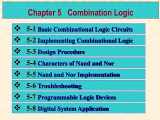
Combination Logic. Chapter 5. AND-OR Logic. AND-OR-Invert Logic. Exclusive-OR logic. Exclusive-NOR Logic. Implementing Combinational Logic from a Truth Table. Collect minterms to form Some of Products (SOP). Universal Property of NAND and NOR Gates.

Combination Logic
E N D
Presentation Transcript
Combination Logic Chapter 5
Implementing Combinational Logic from a Truth Table Collect minterms to form Some of Products (SOP)
Universal Property of NAND and NOR Gates The NAND is a universal gate because it can be used to produce the NOT, the AND, the OR, and the NOR functions. The NOR gate is a universal gate because it can produce the NOT, AND, OR, and NAND functions.
Figure 5-18NAND logic for X = AB + CD. NAND-NAND SOP
Development of the AND-OR Equivalent of the Circuit in Figure 5-18. Figure 5--19 NAND negative-OR
Dual Symbols in aNAND Logic DiagramFigure 5--20 NAND is replaced with negative-OR
Figure 5-24NOR logic for X = (A + B)(C + D). NOR-NOR POS
Figure 5-25 Dual Symbols of NOR NOR negative-AND
Dual Symbols in aNOR Logic DiagramFigure 5--26 NOR is replaced by a negative-AND
Programmable Logic: CPLDs • A CPLD basically consists of multiple groups of PAL / GAL-like arrays • Each PAL/GAL group is called a logic array block (LAB), function block, or some similar term • Each logic array block contains a number of PAL/GAL-like arrays called macrocells • Each LAB can be interconnected with other LAB or to other I/Os using programmable interconnect array (PIA) • The CPLD uses sum-of-produces architecture • Most CPLDs use E2CMOS technology
Logic Array Block (LAB) • Each logic array block in a CPLD contains several macrocells • 32 to several hundred macrocells in one LAB • A macrocell has and AND array, a product-term select matrix, an OR gate, and a programmable register section
Each macrocell has • A fixed number of AND gates feeding the product term selection matrix (AND array) • A product-term expander where inputs from other macrocells allow more product terms • A product-term expander output will provide any selected product term to other macrocells in the LAB or other Lab via the PIA • An OR gate • A programmable register (flip-flop)
Programmable Interconnect Array (PIA) • Consists of connectors that run throughout the CPLD to connect the macrocells in each LAB • The PIA also connects the the AND gate and other elements of the microcells
CPLDs Companies • CPLD architecture is different between companies but all CPLDs are based on PAL/GAL SOP logic arrays • Altera’s MAX 7000 family • Xilinx XC9500 family • Lattice ispXPLD 5000MX, ispMACH 4000
Structural Approach to VHDL Programming • Writing the program as if IC devices were placed on a circuit board and connected with wires • Describe the logic functions and how the connect • VHDL keyword component is used to predefine a logic function for repeated use • VHDL keyword signal is used as a wire is used to connect between components
Structural Approach to VHDL Programming • component keyword • signal keyword
VHDL Components • Predefined logic • Place in a VHDL library and use repeatedly • Similar to a storage bin of IC chips • Any logic function can become a component and used in large programs
VHDL Components component name_of_component is port (port definition); end component name_of_component;
Signals in VHDL • Signals are analogous to wires that connect components • Inputs and outputs are declared in the entity declaration • Signals are declared within the architecture using the signal statement • Signal is a VHDL keyword
Predefined programs for a 2-input AND gate and a 2-input OR gate Figure 5--49 Assume the following gates are predefined:
Example, Figure 5-50 entity AND_OR_Logic is port (IN1, IN2, IN3, IN4: in bit; OUT3: out bit); end entity AND_OR_Logic; architecture LogicOperation of AND_OR_Logic is component AND_gate is port (A, B: in bit; X: out bit); end component AND_gate; component OR_gate is port (A, B: in bit; X: out bit); end component OR_gate; signal OUT1, OUT2: bit; begin G1: AND_gate port map (A=>IN1, B=>IN2, X=>OUT1); G2: AND_gate port map (A=>IN3, B=>IN4, X=>OUT2); G3: OR_gate port map (A=>OUT1, B=>OUT2, X=>OUT3); end architecture LogicOperation;
Figure 5--51Instantiation statements and port mapping applied to the AND-OR logic. Signals are shown in red. Example, Figure 5-51 G1: AND_gate port map (A=>IN1, B=>IN2, X=>OUT1); Read as input A of AND_gate G1 is connected to input IN1, input B of the gate is connected to input IN2, and the output X of the gate is connected to the signal OUT1. G2: AND_gate port map (A=>IN3, B=>IN4, X=>OUT2); G3: OR_gate port map (A=>OUT1, B=>OUT2, X=>OUT3);
VHDL Concurrency • Concurrency permits statements to be processed in parallel (simultaneously) • Concurrency applies to statements between the begin and the end statements entity combinational is port (A, B, C, D: in bit; X, Y: out bit); end entity combinational; architecture Example of Combinational is begin X<=(A and B) or not C; Y<=C or not D; end architecture Example; Concurrent statements: The order in which they appear does not matter. Remember, the hardware gates are processing the inputs in parallel.
VHDL Processes • A process is executed in sequence • Sensitivity list is a list of signals to which the process is sensitive and is optional Name: process (sensitivity list) is Declarations begin Sequential statements end process;
Variables in VHDL • The variable is a type of object that holds data • A VHDL variable can only be used in a process • The variable assignment uses the operator := • Variables are declared between process and begin • Y := B
Example 5-16, Figure 5-53 entity FlightSafety is port (A, B, C, D: in bit; X, Y: out bit); end entity FlightSafety; architecture SensorLogic of FlightSafety is begin process (A, B, C, D) variable V1: bit; V1:=(A and B) or (A and C) or (A and D) or (B and C) or (B and D) or (C and D); X:=V1; --X is assigned the value V1 Y:= not V1; --Y is assigned the value V1 end process; end architecture SensorLogic; By declaring the variable V1, common Boolean expressions need only be described once.
Using Software Development Tools • Enter the VHDL code in to the editor of a software development tool • Test the program using the simulation provided
Figure 5-54A VHDL program for a combinational logic circuit after entry on a typical text editor that is part of a development software tool. Software Development Tools
Figure 5-55A typical waveform editor tool showing the simulated waveforms for the logic circuit described by the VHDL code in Figure 5-54. Software Development Tools
VHDL Components component name_of_component is port (port definition); end component name_of_component; • - 2-input XOR gate component declaration • component XOR_gate is • port (A, B: in bit; X: out bit); • end component XOR-gate The entity XOR_gate and the architecture of the XOR_gate must also be defined
In a library in the entity and architecture of the OR_1 and the XOR_gate -- program for the XOR OR circuit entity XOR_OR_Logic is port (IN1, IN2, IN3, IN4: in bit; OUT3: out bit); end entity XOR_OR_Logic; architecture LogicOperation of XOR_OR_Logic is component XOR_gate is
program for the XOR OR circuit continued architecture LogicOperation of XOR_OR_Logic is component XOR_gate is port (A, B: in bit; X: out bit); end component XOR_gate; component OR_1 is port (A, B; in bit; X: out bit): end component OR_1; signal OUT1, OUT2: bit;
program for the gate XOR OR circuit continued begin G1: XOR_gate port map (A=>IN1, B=>IN2, X=>OUT1); G2: XOR_gate port map (A=>IN3, B=>IN4, X=>OUT2); G3: OR1 port map (A=>OUT1, B=>OUT2, X=>OUT3); end architecture LogicOperation
Functions of Combination Logic Chapter 6