Download
1 / 21
210 likes | 424 Views
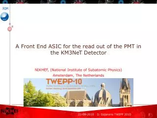
A Front End ASIC for the read out of the PMT in the KM3NeT Detector. NIKHEF, (National Institute of Subatomic Physics) Amsterdam, The Netherlands. Topical Workshop on Electronics for Particle Physics 20-24 September 2010 Aachen, Germany. Contents. Introduction to the KM3NeT Experiment.

E N D
A Front End ASIC for the read out of the PMT in the KM3NeT Detector NIKHEF, (National Institute of Subatomic Physics) Amsterdam, The Netherlands Topical Workshop on Electronics for Particle Physics 20-24 September 2010 Aachen, Germany D. Gajanana TWEPP 2010
Contents • Introduction to the KM3NeT Experiment. • KM3NeT Detector Concept. • Read out electronics. • Specifications of the ASIC. • The Circuit. • Test Results. • Conclusions & Future. D. Gajanana TWEPP 2010
KM3NeT Experiment • Neutrinos are unique messengers from the most violent, highest-energy processes in our Galaxy and far beyond. • Neutrino astronomy is experimentally highly demanding, requiring vast volumes of target material, such as water or ice & dark environment. Toulon (France) Pylos (Greece) Capo Passero (Italy) D. Gajanana TWEPP 2010
KM3NeT Detector concept • The detection of high‐energy muon neutrinos exploits the emission of Cherenkov light by the muon and other charged secondary particles produced in a neutrino interaction. • Photo-Multiplier-Tubes (PMTs) housed in glass spheres (optical modules), are deployed in the deep sea. 320m D. Gajanana TWEPP 2010
Read-Out Electronics 31 ASICs per Optical Module 12+19 Photons P. Timmer’s talk PMT-base BOB Converterboard LVDS Pre-amp Comprtr 2 FPGA S apd 380V ThresholdDAC HV i2c opamp ID Storey-logicboard 12V cpld I2C Decoder + Cntrl i2c 12V osc.1 feedback HVDAC 5V3V3 switch 3V3 (Aux. electr.) switch switch 2 Signalcollectionboard ASIC Aux.electr. D. Gajanana TWEPP 2010
Specifications of the ASIC • Time resolution : 2ns (Photon arrival time accuracy) • Time-over-Threshold : 1pe → 25ns (800 000 e-)..10pe → 350ns (8000000e-) • Number of channels : several hundred thousands. • LVDS signaling. • I2C slow control. • Comparator threshold adjustment: 0…375 000 e- → Vincom= ±200mV Resolution : 8bits (bin size=1500 e- /1.2mV) • Reference voltages for High Voltage circuit: 2.0V …2.8V (resolution 8bits)→ High Voltage: -700V …-1500V • Power consumption : ~ 20mW • Technology: 0.35μm CMOS (AustriaMicroSystems) • Immunity to dirty Power supplies • Immunity to voltage breakdowns originated in the PMT D. Gajanana TWEPP 2010
Contents • Introduction to the KM3NeT Experiment. • KM3NeT Detector Concept. • Read out electronics. • Specifications of the ASIC. • The Circuit. • Test Results. • Conclusions & Future. D. Gajanana TWEPP 2010
Analog Part Bandgap 1.2V DAC settings from I2C DAC output Opamp output Opamp input (HV circuit on PCB) DAC settings from I2C Bias Block + Threshold setting DAC for Comparator HV setting DAC + Opamp for HV feedback Preamp Comparator Buffers LVDS From PMT LVDS Prototyped before D. Gajanana TWEPP 2010
Preamplifier • Two-stage charge preamplifier with RC feedback. 2 photons 1 photon Time-over-Threshold OUT REF. Preamp 1V Time-to-Threshold IN 0.5 mA 125 μA 15kΩ 300 fF D. Gajanana TWEPP 2010
Comparator • Single Stage comparator. OUT Threshold 0.8 – 1.2V IN 375 μA D. Gajanana TWEPP 2010
LVDS Driver 3.5 mA Pbias • Conventional LVDS driver, single stage CMFB circuit. • 3.5mA * 100Ω = 350mV differential signal. Pbias X IN+ IN- CM REF. 1.2V 100k 100k X OUT- OUT+ Nbias 0.5 mA Nbias D. Gajanana TWEPP 2010
Digital Part HV on-off Scan Chain Analog Chain Test Clock Generator ~ 10MHz Clk Enable I2C BUS Data I2C Decoder + PROM Control Logic Burn Enable PROM 20Bits Control POR To DACs VerilogNetlist + SDF files VerilogNetlist VerilogNetlist D. Gajanana TWEPP 2010
Digital Simulations - Example • Post Layout simulations with SDF files (Digital Part only). • Tools Used : Modelsim, ncSim suite, Synopsys. DAC + HV + Control & Test I2C PROM D. Gajanana TWEPP 2010
Analog Bondpad Modifications Previous pad Power supply ripples = ±40mV Vdd Unavoidable – From HV Supply on PCB ~0.23pF Internal Circuitry Power Clamp I/O Gnd Possible Solution Problem Vdd Internal Circuitry Power Clamp Time jitter on the falling edge I/O Gnd Present pad D. Gajanana TWEPP 2010
Layout & Integration 1.8 mm Comparator + Buffers Preamp Clock Genrtr POR LVDS Bandgap PROM I2C Decoder + PROM Control HV Control Block Bias Block D. Gajanana TWEPP 2010
Mixed-Signal Simulation Results • Post Layout including Bondpads simulations. • Tools Used : AMS environment (Ultrasim/spectre and ncSim suite). I2C Comparator DAC HV DAC LVDS D. Gajanana TWEPP 2010
Test Setup • Preliminary tests only. • 3 samples packaged and tested. • I2C communication successful. • DAC settings changeable. • Analog chain functional. D. Gajanana TWEPP 2010
Test Results 2 photons 1 photon Time-to-Threshold Time walk=3 ns D. Gajanana TWEPP 2010
Test Results 2 photons 1 photon Time-over-Threshold D. Gajanana TWEPP 2010
Conclusions & Future • An ASIC to read out the PMT was successfully designed, simulated, fabricated and tested. • Preliminary “Test results” are satisfactory & in line with simulation results and future functionality is being tested. • More intensive tests need to be performed on the ASIC. • We aim an engineering run during Q1 of 2011, allowing for a production ramp-up in Q1 of 2012. D. Gajanana TWEPP 2010
Thank You • KM3NeT project team, V. Gromov, Eric Heine, RuudKluit, John Hug, Jan-Willem Schmelling, P. Jansweijer, V. Zivkovic, P. Timmer, JoopRovekamp, ET colleagues at NIKHEF. References • www.km3net.org/CDR/CDR-KM3NeT.pdf • www.km3net.org/TDR/Prelim-TDR-KM3NeT.pdf • Prof. Sansen “Analog Design Essentials” Springer, 2006. • Chang ZY, Sansen W. “Low-noise wide band amplifiers in Bipolar and CMOS technologies” Springer, 1996. • Tajalli et. al. “A Slew Controlled LVDS Output Driver Circuit in 0.18 μm CMOS Technology”, JSSC, Feb. 2009. • www.national.com/LVDS • J.Vandenbussche et. al. “A fully integrated Low-Power CMOS Particle Detector Front-End for space applications”, IEEE Trans. on Nuclear Science, Aug. 1998. D. Gajanana TWEPP 2010