Download
1 / 24
240 likes | 446 Views
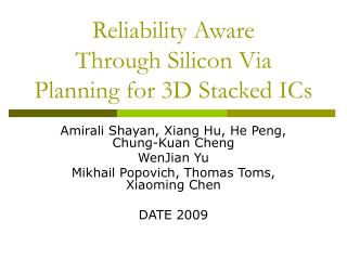
Reliability Aware Through Silicon Via Planning for 3D Stacked ICs. Amirali Shayan, Xiang Hu, He Peng, Chung-Kuan Cheng WenJian Yu Mikhail Popovich, Thomas Toms, Xiaoming Chen DATE 2009. Outline. Introduction Reliability of Through Silicon Vias Problem Formulation 3D PDN Analysis Flow

E N D
Reliability Aware Through Silicon Via Planning for 3D Stacked ICs Amirali Shayan, Xiang Hu, He Peng, Chung-Kuan Cheng WenJian Yu Mikhail Popovich, Thomas Toms, Xiaoming Chen DATE 2009
Outline • Introduction • Reliability of Through Silicon Vias • Problem Formulation • 3D PDN Analysis Flow • Results and Analysis • Conclusion
Outline • Introduction • Reliability of Through Silicon Vias • Problem Formulation • 3D PDN Analysis Flow • Results and Analysis • Conclusion
Introduction • 3D integration technology is one of the fastest growing IC design directions that offer flexible and low cost integration and packaging solutions • The 3D PDN (Power Delivery Network) features bring in new challenges • The reliability of the network • The signal integrity • The increase in the power density • The distance of the stacked dice from heat sink will increase the temperature profile
Introduction • In this work, a framework for the analysis of the reliability of 3D PDN under local TSV failures is proposed • The model is first solved in frequency domain to identify the behavior of the system • Then the time domain voltage noise under worse case transistor switching currents is obtained with our enhanced vector fitting algorithm
Introduction • The objective of the optimization is to increase the reliability of the 3D structure and reduce the voltage noise while minimizing the block out area from TSV design rules
Outline • Introduction • Reliability of Through Silicon Vias • Problem Formulation • 3D PDN Analysis Flow • Results and Analysis • Conclusion
Reliability of Through Silicon Vias • Reliability?? • As the technology shrinks, vias become more and more sensitive. When the via fails to make proper connection, unwanted loss in yield and performance may occur • Efficient via placement is necessary
Outline • Introduction • Reliability of Through Silicon Vias • Problem Formulation • 3D PDN Analysis Flow • Results and Analysis • Conclusion
Problem Formulation • In this TSV reliability analysis, three major metrics are used: • Maximum power noise voltage drop (ΔV ) [6] • Reliability factor ( R ) [5] • Block out area ( Ablockout ) • Cost function
Outline • Introduction • Reliability of Through Silicon Vias • Problem Formulation • 3D PDN Analysis Flow • Results and Analysis • Conclusion
3D PDN Analysis Flow • Skin effect
3D PDN Analysis Flow • In order to convert the frequency domain results into time domain we use vector fitting method [7] • However, as the clock frequency of the 3D stacked ICs is reaching GHz range and the transistor current stimuli includes many high frequency components, conventional vector fitting method [7] cannot fits high frequency component properly and the time domain recovered result has a large error
3D PDN Analysis Flow • This work enhanced the vector fitting process and use the remainder of the vector fitting as the next iteration input and perform the vector fitting process iteratively until reaches the acceptable error boundary (in our test case )
Outline • Introduction • Reliability of Through Silicon Vias • Problem Formulation • 3D PDN Analysis Flow • Results and Analysis • Conclusion
Results and Analysis • TSV dimension and density scaling
Results and Analysis • TSV dimension and density scaling
Results and Analysis • Reliability of the TSV
Results and Analysis • TSV analysis framework
Outline • Introduction • Reliability of Through Silicon Vias • Problem Formulation • 3D PDN Analysis Flow • Results and Analysis • Conclusion
Conclusion • In this work, a reliability aware through silicon via analysis framework is proposed • The design parameters of the TSV and the 3D PDN are analyzed to mitigate the increase in the power noise caused by the TSV local failure