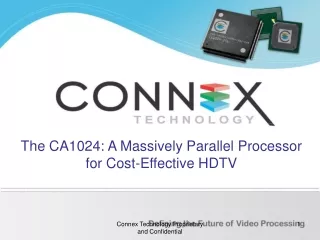
3D-MAPS: Massively Parallel Processor with Stacked Memory
Explore the groundbreaking 3D-MAPS technology, showcasing a highly efficient processor design with stacked memory. This innovative approach offers advantages in power efficiency, footprint, and bandwidth compared to traditional 2D architectures.

3D-MAPS: Massively Parallel Processor with Stacked Memory
E N D
Presentation Transcript
ISSCC2012 Major Reference: 3D-MAPS: 3D Massively Parallel Processor with Stacked Memory Dae Hyun Kim, KritAthikulwongse, Michael Healy, Mohammad Hossain, MoongonJung, et al. Georgia Institute of Technology, Atlanta, GA KAIST, Daejeon, Korea Amkor Technology, Seoul, Korea University of Tehran CIDSP Seminar May 2013 Presented by: S.Ghanbari
2-D Ics[7]: • Large Chip Area • Long Interconnects Causing Delay-related Issues • Hard to Meet Different Voltage Requirements • Inability of Using Incompatible Technologies Together 2D vsSoCvs 3D[7]
Solutions[7] • 3D Packaging Stacking several chips in one package. Chips communicate using off-chip signaling. • 3D Ics[7] Using different layers on the same chip. Chips communicate using on-chip signaling. 3D IC has the same relation with a 3D package as SoC with a Circuit board.
3D IC Advantages[7] • Footprint • Cost(yield and fabrication cost) • Integrating different processes, better optimization • Shorter interconnect • Power reduction with On-chip signals • Circuit security • Bandwidth
Manufacturing Technologies[7] • Wafer-on-Wafer • Die-on-Wafer • Die-on-Die Design styles[7] • Gate-level Integration • Block-level Integration
3D-MAPS 3D Massively Parallel Processor with Stacked Memory • 64 general-purpose processor cores at 277MHz • 256KB SRAM • 130nm Technology • 33M Transistors, 50K TSV, 50K Face-to-Face connections in 5mm*5mm footprint. • 1.5V Supply, up to 4W power consumption. Results in 16W/cm2 power density.
3D-MAPS 3D Massively Parallel Processor with Stacked Memory • 64 custom processor cores • 4KB SRAM data memory for each core • Theoretical maximum data memory bandwidth at 277MHz is 70.9GB/s Overview and single core architecture[1]
3D-MAPS Tezzaron 3D Technology • F2F(Face to Face) bonding • 235 I/O cells along the periphery of the core die. • 204 TSVs, connecting metal 1 to backside metal, wirebonded to the package. • Uses dummy TSVs to satisfy the TSV density rule(Total of 4500 dummy TSVs on the memory die).
3D-MAPS Stacking, TSV, F2F, and chip-to-package connection[1]
3D-MAPS 294 P/G land pads to supply high current(2.7A) hence high temperature(~90C from simulation). Heat and Power measures • A dummy silicon substrate to increase thermal conductivity. • Center region of LGA implemented as a large copper pad dedicated to VSS to decrease thermal resistance. • Decoupling capacitors added to improve power integrity. Average parasitic values of signal package routes: R=377.5mΩ L=4.1nH C=1pF
3D-MAPS Bandwidth and power measurement results[1]
3D-MAPS Frequency vs. power (at 1.5V) and voltage vs. power (at 250MHz) for AES encryption[1]
3D-MAPS Regularity Single core and memory tile layouts[1] Modularity Die photos[1]
3D-MAPS References: [1] DaeHyun Kim, KritAthikulwongse, Michael Healy, Mohammad Hossain, Moongon Jung, et al. “3D-MAPS: 3D Massively Parallel Processor with Stacked Memory”, ISSCC 2012, S.10, P.06. " [2] M. Koyanagi, et al. “Neuromorphic Vision Chip Fabricated Using Three-Dimensional Integration Technology”, ISSCC Dig. Tech. Papers, pp. 270-271, 2001. [3] U. Kang, et al. “8Gb 3D DDR3 DRAM Using Through-Silicon-Via Technology”, ISSCC Dig. Tech. Papers,pp. 130-131, 2009. [4] G. Van der Plas, et al., “Design Issues and Considerations for Low-Cost 3D TSV IC Technology”, ISSCC Dig. Tech. Papers,pp. 148-149, 2010.. [5J.-S. Kim, et al. “A 1.2V 12.8GB/s 2Gb Mobile Wide-I/O DRAM with 4x128 I/OsUsing TSV-Based Stacking”, ISSCC Dig. Tech. Papers,pp. 496-498, 2011. [6] M. Healy, et al. ”Design and Analysis of 3D-MAPS: A Many-Core 3D Processor with Stacked Memory”, IEEE Custom Integrated Circuits Conf., pp. 1-4, 2010. [7] http://en.wikipedia.org/wiki/Three-dimensional_integrated_circuit