Download
1 / 32
320 likes | 474 Views
Integrated Interlayer Via Planning and Pin Assignment for 3D ICs. Xu He, Sheqin Dong, Xianlong Hong, Satoshi Goto SLIP ’ 09. OUTLINE. Introduction Problem Formulation Pin Assignment and Interlayer Via Planning for One Block (PAVPO) Pin Assignment and Interlayer Via Planning (PAVP)

E N D
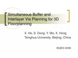
Integrated Interlayer Via Planning and Pin Assignment for 3D ICs Xu He, Sheqin Dong, Xianlong Hong, Satoshi Goto SLIP’09
OUTLINE • Introduction • Problem Formulation • Pin Assignment and Interlayer Via Planning for One Block (PAVPO) • Pin Assignment and Interlayer Via Planning (PAVP) • Experimental Results • Conclusion and Future Work
OUTLINE • Introduction • Problem Formulation • Pin Assignment and Interlayer Via Planning for One Block (PAVPO) • Pin Assignment and Interlayer Via Planning (PAVP) • Experimental Results • Conclusion and Future Work
Introduction • With the persistent shrinking of device size and increasing of integration density, interconnection delay has become one of the most important issues in VLSI design • 3D ICs, which are composed of several separate device layers connected by short and vertical interlayer interconnections, can significantly reduce the interconnect delay and achieve high circuit performance
Introduction • In 3D ICs, the nets which cross multiple layers need vertical interlayer interconnections • However, unlike the regular via (pitch≦0.5μm×0.5μm) located in metal layers, the interlayer via is very large (pitch≒5μm×5μm), and is usually placed at the whitespace between the macro blocks in the device layer
Introduction • As far as many researches we known, there is no existing work that considers pin assignment during interlayer via planning • If interlayer via planning process is integrated with pin assignment, the location of interlayer via will be much more flexible and the wire length will be further reduced
Contribution • First consider simultaneous pin assignment and interlayer via planning for the two-pin nets connecting one source block to all its sink blocks • Min-cost maximum flow based algorithm runs in polynomial time • The process can be considered in many steps of physical design, such as during or after floorplanning or placement, or during global routing
OUTLINE • Introduction • Problem Formulation • Pin Assignment and Interlayer Via Planning for One Block (PAVPO) • Pin Assignment and Interlayer Via Planning (PAVP) • Experimental Results • Conclusion and Future Work
Problem Formulation • Problem • Pin assignment and interlayer via planning for 3D ICs • Objective • Interlayer via of multi-layer net can be located as successfully as possible while total wire length is minimized • Input • A 3D floorplan, net list the available pin locations of blocks • Output • The final pin position of each net, interlayer via locations of multi-layer nets
Problem Formulation • Basic assumptions • All the macro blocks are hard ones • All the nets are two-pin nets, and multi-pin nets are split into a set of two-pin nets • Interlayer via can only be inserted into whitespace • A net cannot cross the same device layer more than once
OUTLINE • Introduction • Problem Formulation • Pin Assignment and Interlayer Via Planning for One Block (PAVPO) • Pin Assignment and Interlayer Via Planning (PAVP) • Experimental Results • Conclusion and Future Work
Pin Assignment and Interlayer Via Planning for One Block (PAVPO) • Algorithm PAVPO (B, N, P) • Divide the 3D layout into grid, and calculate the capacity of interlayer via in each grid node region • Construct the network graph G(V, E), assign cost and capacity for each edge • Use min-cost maximum flow algorithm on G(V, E) • Get the pin positions and interlayer via locations for each net according to the flow
PAVPO (Second Step) • G(V, E) • V = {s, t, t1, …, tn}∪P∪GN • E = Es∪Et∪Eg∪Ev∪Epg∪Ept, where • Es: from s to all pin positions of Ps • Et: from subsink node ti(i=1,…,n) to t • Eg: the grid edges of each layer • Ev: edge between upper layer grid node and its corresponding grid node in the lower adjacent • Epg: edges between the pin positions of Pi(i=s, 1,…, n) and their nearby grid node • Ept: from the pins of Pi(i=1, …, n) to ti
PAVPO (Second Step) • Capacity of edge • For edges in Es∪Epg∪Ept, the capacity is 1 • For edges (ti, t) in Et, the capacity is equal to |Ni|(i=1,…,n) • For edges in Ev, the capacity is the upper layer grid node’s interlayer via capacity • For edges in Eg, the capacity has no constraint, and we set the capacity infinite
PAVPO (Second Step) • Cost of edge • For edges in Es∪Et∪Ev∪Ept, the cost is zero • The cost of edges in Eg∪Epg is according to the Manhattan distance of the two vertexes
OUTLINE • Introduction • Problem Formulation • Pin Assignment and Interlayer Via Planning for One Block (PAVPO) • Pin Assignment and Interlayer Via Planning (PAVP) • Experimental Results • Conclusion and Future Work
Decompose Multi-pin Net • First, we build a complete graph • Then we use Prim’s algorithm to get the minimum spanning tree • Problem
The Solution Block s Block 1 Block 2
Pin Assignment and Interlayer Via Planning (PAVP) • Algorithm PAVP • Increase the amount of available pin positions in each block • For each block, apply PAVPO(B, N, P) algorithm • Get pin’s final positions by using pin mapping process on every block, and update wire length of corresponding net
OUTLINE • Introduction • Problem Formulation • Pin Assignment and Interlayer Via Planning for One Block (PAVPO) • Pin Assignment and Interlayer Via Planning (PAVP) • Experimental Results • Conclusion and Future Work
OUTLINE • Introduction • Problem Formulation • Pin Assignment and Interlayer Via Planning for One Block (PAVPO) • Pin Assignment and Interlayer Via Planning (PAVP) • Experimental Results • Conclusion and Future Work
Conclusion and Future Work • In this paper, we have addressed the issue of simultaneous interlayer via planning and pin assignment which is new for 3D • Experimental results have shown that our algorithm can effectively optimize the total wire length and interlayer via amount • Thermal analysis of interlayer via will be discussed in the future work