VLSI-Design
0 likes | 160 Views
IC Technology-MOS, PMOS, NMOS, CMOS & BiCMOS:<br>Mooreu2019s Law:

VLSI-Design
E N D
Presentation Transcript
UNIT-I Introduction to IC Technology-MOS, PMOS, NMOS, CMOS & BiCMOS: Moore’s Law: Gordon Moore: co-founder of Intel Predicted that the number of transistors per chip would grow exponentially (double every 18 months) Exponential improvement in technology is a natural trend: –e.g. Steam Engines - Dynamo - Automobile The Cost of Fabrication: •Current cost $2 - 3 billion •Typical fab line occupies 1 city block, employees a few hundred employees •Most profitable period is first 18 months to 2 years •For large volume IC’s packaging and testing is largest cost •For low volume IC’s, design costs may swamp manufacturing costs What is a Silicon Chip? •A pattern of interconnected switches and gates on the surface of a crystal of semiconductor (typically Si) •These switches and gates are made of –areas of n-type silicon –areas of p-type silicon –areas of insulator –lines of conductor (interconnects) joining areas together •Aluminium, Copper, Titanium, Molybdenum, polysilicon, tungsten • The geometryof these areas is known as the layout of the chip •Connections from the chip to the outside world are made around the edge of the chip to facilitate connections to other devices Switches: •Digital equipment is largely composed of switches •Switches can be built from many technologies –relays (from which the earliest computers were built) –thermionic valves –transistors •The perfect digital switch would have the following: –switch instantly –use no power –have an infinite resistance when off and zero resistance when on •Real switches are not like this! Semiconductors and Doping: •Adding trace amounts of certain materials to semiconductors alters the crystal structure and can change their electrical properties –in particular it can change the number of free electrons or holes •N-Type –semiconductor has free electrons
–dopant is (typically) phosphorus, arsenic, antimony •P-Type –semiconductor has free holes –dopant is (typically) boron, indium, gallium •Dopants are usually implanted into the semiconductor using Implant Technology, followed by thermal process to diffuse the dopants IC Technology: •Speed / Power performance of available technologies •The microelectronics evolution •SIA Roadmap •Semiconductor Manufacturers 2001 Ranking Metal-oxide-semiconductor (MOS) and related VLSI technology: •pMOS •nMOS •CMOS •BiCMOS •GaAs Basic MOS Transistors: •Minimum line width •Transistor cross section •Charge inversion channel •Source connected to substrate •Enhancement vs Depletion mode devices •pMOS are 2.5 time slower than nMOS due to electron and hole mobilities • Fabrication Technology: •Silicon of extremely high purity –chemically purified then grown into large crystals •Wafers –crystals are sliced into wafers –wafer diameter is currently 150mm, 200mm, 300mm –wafer thickness <1mm –surface is polished to optical smoothness •Wafer is then ready for processing •Each wafer will yield many chips –chip die size varies from about 5mmx5mm to 15mmx15mm –A whole wafer is processed at a time •Different parts of each die will be made P-type or N-type (small amount of other atoms intentionally introduced - doping -implant) •Interconnections are made with metal
•Insulation used is typically SiO2. SiN is also used. New materials being investigated (low-k dielectrics) •nMOS Fabrication •CMOS Fabrication •p-well process •n-well process •twin-tub process •All the devices on the wafer are made at the same time •After the circuitry has been placed on the chip •the chip is overglassed (with a passivation layer) to protect it •only those areas which connect to the outside world will be left uncovered (the pads) •The wafer finally passes to a test station •test probes send test signal patterns to the chip and monitor the output of the chip •The yield of a process is the percentage of die which pass this testing •The wafer is then scribed and separated up into the individual chips. These are then packaged •Chips are ‘binned’ according to their performance • CMOS Technology: •First proposed in the 1960s. Was not seriously considered until the severe limitations in power density and dissipation occurred in NMOS circuits •Now the dominant technology in IC manufacturing •Employs both pMOS and nMOS transistors to form logic elements •The advantage of CMOS is that its logic elements draw significant current only during the transition from one state to another and very little current between transitions - hence power is conserved. •In the case of an inverter, in either logic state one of the transistors is off. Since the transistors are in series, (~ no) current flows. •See twin-well cross sections BiCMOS: •A known deficiency of MOS technology is its limited load driving capabilities (due to limited current sourcing and sinking abilities of pMOS and nMOS transistors. •Bipolar transistors have –higher gain –better noise characteristics –better high frequency characteristics • BiCMOS gates can be an efficient way of speeding up VLSI circuits •See table for comparison between CMOS and BiCMOS •CMOS fabrication process can be extended for BiCMOS
•Example Applications –CMOS - Logic –BiCMOS –ECL - critical high speed parts of the system - I/O and driver circuits TECHNOLOGIES: Semiconductor Fabrication Processes Starting with an uniformly doped silicon wafer, the fabrication of integrated circuits (IC's) needs hundreds of sequential process steps. The most important process steps used in the semiconductor fabrication are a) Lithography Lithography is used to transfer a pattern from a photomask to the surface of the wafer. For example the gate area of a MOS transistor is defined by a specific pattern. The pattern information is recorded on a layer of photoresist which is applied on the top of the wafer. The photoresist changes its physical properties when exposed to light (often ultraviolet) or another source of illumination (e.g. X-ray). The photoresist is either developed by (wet or dry) etching or by conversion to volatile compounds through the exposure itself. The pattern defined by the mask is either removed or remained after development, depending if the type of resist is positive or negative. For example the developed photoresist can act as an etching mask for the underlying layers. b) Etching Etching is used to remove material selectively in order to create patterns. The pattern is defined by the etching mask, because the parts of the material, which should remain, are protected by the mask. The unmasked material can be removed either by wet (chemical) or dry (physical) etching. Wet etching is strongly isotropic which limits its application and the etching time can be controlled difficultly. Because of the so-called under-etch effect, wet etching is not suited to transfer patterns with sub-micron feature size. However, wet etching has a high selectivity (the etch rate strongly depends on the material) and it does not damage the material. On the other side dry etching is highly anisotropic but less selective. But it is more capable for transfering small structures. c) Deposition A multitude of layers of different materials have to be deposited during the IC fabrication process. The two most important deposition methods are the physical vapor deposition (PVD) and the chemical vapor deposition (CVD). During PVD accelerated gas ions sputter particles from a sputter target in a low pressure plasma chamber. The principle of CVD is a chemical reaction of a gas mixture on the substrate surface at high temperatures. The need of high temperatures is the most restricting factor for applying CVD. This problem can be avoided with plasma enhanced chemical vapor deposition (PECVD), where the chemical reaction is enhanced with radio frequencies instead of high temperatures. An important aspect for this
technique is the uniformity of the deposited material, especially the layer thickness. CVD has a better uniformity than PVD. d) Chemical Mechanical Planarization Processes like etching, deposition, or oxidation, which modify the topography of the wafer surface lead to a non-planar surface. Chemical mechanical planarization (CMP) is used to plane the wafer surface with the help of a chemical slurry. First, a planar surface is necessary for lithography due to a correct pattern transfer. Furthermore, CMP enables indirect pattering, because the material removal always starts on the highest areas of the wafer surface. This means that at defined lower lying regions like a trench the material can be left. Together with the deposition of non-planar layers, CMP is an effective method to build up IC structures. e) Oxidation Oxidation is a process which converts silicon on the wafer into silicon dioxide. The chemical reaction of silicon and oxygen already starts at room temperature but stops after a very thin native oxide film. For an effective oxidation rate the wafer must be settled to a furnace with oxygen or water vapor at elevated temperatures. Silicon dioxide layers are used as high- quality insulators or masks for ion implantation. The ability of silicon to form high quality silicon dioxide is an important reason, why silicon is still the dominating material in IC fabrication. OXIDATION TECHNIQUES 1.Cleaned wafers are placed in the wafer load station where dry nitrogen (N2) is introduced into the chamber. The nitrogen prevents oxidation from occurring while the furnace reaches the required temperature. 2.Once the specified temperature in the chamber is reached, the nitrogen gas flow is shut off and oxygen (O2) is added to the chamber. The source of the oxygen can be gas or water vapor depending upon the dry process or wet process. •After the oxidation is complete and the oxide layer is the correct thickness, nitrogen is reintroduced into the chamber to prevent further oxidation from occurring. •The wafers are then removed from the chamber. After inspection, they are ready for further processing. •Thermal oxidation can be either a dry or a wet process f) Ion Implantation Ion implantation is the dominant technique to introduce dopant impurities into crystalline silicon. This is performed with an electric field which accelerates the ionized atoms or molecules so that these particles penetrate into the target material until they come to rest because of interactions with the silicon atoms. Ion implantation is able to control exactly the distribution and dose of the dopants in silicon, because the penetration depth depends on the kinetic energy of the ions which is proportional to the electric field. The dopant dose can be controlled by varying the ion source. Unfortunately, after ion implantation the crystal structure is damaged which implies worse electrical properties. Another problem is that the implanted dopants are electrically inactive, because they are situated on interstitial sites.
Therefore after ion implantation a thermal process step is necessary which repairs the crystal damage and activates the dopants. g) Diffusion Diffusion is the movement of impurity atoms in a semiconductor material at high temperatures. The driving force of diffusion is the concentration gradient. There is a wide range of diffusivities for the various dopant species, which depend on how easy the respective dopant impurity can move through the material. Diffusion is applied to anneal the crystal defects after ion implantation or to introduce dopant atoms into silicon from a chemical vapor source. In the last case the diffusion time and temperature determine the depth of dopant penetration. Diffusion is used to form the source, drain, and channel regions in a MOS transistor. But diffusion can also be an unwanted parasitic effect, because it takes place during all high temperature process steps. Basic MOS Transistors: Why the name MOS? We should first understand the fact that why the name Metal Oxide Semiconductor transistor, because the structure consists of a layer of Metal (gate), a layer of oxide (Sio2) and a layer of semiconductor.Figure 3 below clearly tell why the name MOS We have two types of FETs. They are Enhancement mode and depletion mode transistor. Also we have PMOS and NMOS transistors. In Enhancement mode transistorchannel is going to form after giving a proper positive gate voltage. We have NMOS and PMOS enhancement transistors. In Depletion mode transistorchannel will be present by the implant. It can be removed by giving a proper negative gate voltage. We have NMOS and PMOS depletion mode transistors.
N-MOS enhancement mode transistor:- This transistor is normally off. This can be made ON by giving a positive gate voltage. By giving a +ve gate voltage a channel of electrons is formed between source drain. P-Mos enhancement mode transistors:-This is normally on. A Channel of Holes can be performed by giving a –ve gate voltage. In P-Mos current is carried by holes and in N-Mos its by electrons. Since the mobility is of holes less than that of electrons P-Mos is slower.
N-MOS depletion mode transistor:- This transistor is normally ON, even with Vgs=0. The channel will be implanted while fabricating, hence it is normally ON. To cause the channel to cease to exist, a –ve voltage must be applied between gate and source.
The process starts with the oxidation of the silicon substrate (Fig. 9(a)), in which a relatively thick silicon dioxide layer, also calledfield oxide, is created on the surface (Fig. 9(b)). Then, the field oxide is selectively etched to expose the silicon surface on which the MOS transistor will be created (Fig. 9(c)). Following this step, the surface is covered with a thin, high-quality oxide layer, which will eventually form the gate oxide of the MOS transistor (Fig. 9(d)). On top of the thin oxide, a layer of polysilicon (polycrystalline silicon) is deposited (Fig. 9(e)). Polysilicon is used both as gate electrode material for MOS transistors and also as an interconnect medium in silicon integrated circuits. Undoped polysilicon has relatively high resistivity. The resistivity of polysilicon can be reduced, however,by doping it with impurity atoms. After deposition, the polysilicon layer is patterned and etched to form the interconnects and the MOS transistor gates (Fig. 9(f)). The thin gate oxide not covered by polysilicon is
also etched away, which exposes the bare silicon surface on which the source and drain unctions are to be formed (Fig. 9(g)). The entire silicon surface is then doped with a high concentration of impurities, either through diffusion or ion implantation (in this case with donor atoms to produce n-type doping). Figure 9(h) shows that the doping penetrates the exposed areas on the silicon surface, ultimately creating two n-type regions (source and drain junctions) in the p-type substrate. The impurity doping also penetrates the polysilicon on the surface, reducing its resistivity. Note that the polysilicon gate, which is patterned before doping actually defines the precise location of the channel region and, hence, the location of the source and the drain regions. Sincethis procedure allows very precise positioning of the two regions relative to the gate, it is also called the self-aligned 8process. Once the source and drain regions are completed, the entire surface is again covered with an insulating layer of silicon dioxide(Fig. 9 (i)). The insulating oxide layer is then patterned in order to provide contactwindows for the drain and source junctions (Fig. 9 (j)). The surface is covered withevaporated aluminum which will form the interconnects (Fig. 9 (k)). Finally, the metal layer is patterned and etched, completing the interconnection of the MOS transistors on the surface (Fig. 9 (l)). Usually, a second (and third) layer of metallic interconnect can also be added on top of this structure by creating another insulating oxide layer, cutting contact (via) holes, depositing, and patterning the metal. CMOS fabrication: When we need to fabricate both nMOS and pMOS transistors on the same substrate we need to follow different processes. The three different processes are,P-well process ,N-well process and Twin tub process.
P-WELL PROCESS: The p-well process starts with a n type substrate. The n type substrate can be used to implement the pMOS transistor, but to implement the nMOS transistor we need to provide a p-well, hence we have provided heplace for both n and pMOS transistor on the same n-type substrate. Mask sequence. Mask 1 defines the areas in which the deep p-well diffusion takes place. Mask 2: It defines the thin oxide region (where the thick oxide is to be removed or
stripped and thin oxide grown) Mask 3: It’s used to pattern the polysilicon layer which is deposited after thin oxide. Mask 4: A p+ mask (anded with mask 2) to define areas where p-diffusion is to take place. Mask 5: We are using the –ve form of mask 4 (p+ mask) It defines where n-diffusion is to take place. Mask 6: Contact cuts are defined using this mask. Mask 7: The metal layer pattern is defined by this mask. Mask 8: An overall passivation (overglass) is now applied and it also defines openings for accessing pads. The cross section below shows the CMOS pwell inverter. Twin-tub process: Here we will be using both p-well and n-well approach. The starting point is a n- type material and then we create both n-well and p-well region. To create the both well we first go for the epitaxial process and then we willcreate both wells on the same substrate.
Bi-CMOS technology: - (Bipolar CMOS) The driving capability of MOS transistors is less because of limited current sourcing and sinking capabilities of the transistors. To drive large capacitive loads we can think of Bi- Cmos technology. This technology combines Bipolar and CMOS transistors in a single integrated circuit, by retaining benefits of bipolar and CMOS, BiCMOS is able to achieve VLSI circuits with speed-power-density performance previously unattainable with either technology individually. Characteristics of CMOS Technology • Lower static power dissipation • Higher noise margins • Higher packing density – lower manufacturing cost per device • High yield with large integrated complex functions • High input impedance (low drive current) • Scaleable threshold voltage • High delay sensitivity to load (fan-out limitations) • Low output drive current (issue when driving large capacitive loads) • Low transconductance, wheretransconductance, gm αVin • Bi-directional capability (drain & source are interchangeable) • A near ideal switching device Characteristics of Bipolar Technology • Higher switching speed • Higher current drive per unit area, higher gain • Generally better noise performance and better high frequency characteristics • Better analogue capability • Improved I/O speed (particularly significant with the growing importance of package limitations in high speed systems). • high power dissipation • lower input impedance (high drive current) • low voltage swing logic • low packing density • low delay sensitivity to load • high gm (gm αVin) • high unity gain band width (ft) at low currents • essentially unidirectional
From the two previous paragraphs we can get a comparison between bipolar and CMOS technology. The diagram given below shows the cross section of the BiCMOS process which uses an npn transistor.
BASIC ELECTRICAL PROPERITIES: 1. Linear Region: Figure 1. Concentration Contours in Linear Region. A uniform narrow channel exists. KVL: VG - VS = VG VC + VC - VS VG - VS = VGS VG - VC = VGC VC - VS = V (x) VGS = VGC + V (x) or VGS - V (x) = VGC
2. Saturation Region When VDS _ (VGS - VTH) channel pinches off. This means that the channel current near the drain spreads out and the channel near drain can be approximated as the depletion region. After this occurs, at VDS = (VGS - VTH), if you make VDS larger, the current ID does not change (to zero approximation). This is because any additional VDS you add will get dropped across the depletion region and won't change the current ID. So for VDS _ (VGS - VTH) we _nd ID by setting VDS = (VGS - VTH) substituting into the linear equation.
Transconductance: Transconductance is a property of certain electronic components. Conductance is the reciprocal of resistance; transconductance is the ratio of the current change at the output port to the voltage change at the input port. It is written as gm. For direct current, transconductance is defined as follows: For small signal alternating current, the definition is simpler:
MOStransistor theory Introduction: A MOS transistor is a majority-carrier devi ce, in which the current in a conducting channel between the source andthe drain is modulated by a voltage appli ed to the gate. NMOS(n-type MOStransistor): (1)Majority carrier = electrons (2)A positive voltage applied on the gate with respect to the substrate enhances the number of electrons in the channel and hence increases the conductivity of the channel. (3)If gate voltage is less than a threshold voltage Vt, the channel i s cut-off (very low current between source & drain). PMOS(p-type M OStransistor): (1)Majority carrier = holes (2)App lied voltage is negative with respect to substrate. Relationship between Vgs and Ids, for a fixed Vds: MOSequations (Basic DCequations): Three MOS operating regions are: Cutoff or subthreshold region, linear region and saturation region. The followingequation describes all these three regions:
Where βis MOS transistor gain and it is given by β =μ ε/tox (W/L) μ‘is the mobility of the charge carrier εis the permitivity of the oxide layer. Tox is the thickness of the oxide layer. W is the width of the transistor.( shown in diagram) L is the channel length of the transistor. (shown in diagram) Second Order Effects: Following are the list of second order effects of MOSFET: Threshold voltage –Body effect Sub-threshold region
Channel length modulation Mobility variation Fowler_Nordheim Tunneling Drain Punch-through Impact Ionization –Hot Electrons Threshold voltage –Bodyeffect The change in the threshold voltage of a MOSFET, because of the voltage difference between body and source is called body effect. The expression for the threshold voltage is given by the following expression. If Vsb is zero, then Vt= Vt(0) that means the value of the threshold voltage will not be changed. Therefore, weshort circuit the source and substrate so that, Vsb will be zero. Sub-threshold region: For Vgs<Vtalso wewill get some value of Drain current this is called as Subthreshold current And the region is called as Sub-threshold region. Channel length modulation: The channel length o f the MOSFET is changed due to the change in the drain to source voltage. This effect is called as the channel length modulation. The effective channel length & the value of the drain current considering channel length modulation into effect is given by, Where λi s the channel length modulation factor. Mobility: Mobility is the defined as the ease with which the charge carriers drift in the substrate material .
Mobility decreases with increase in doping concentration and increase in temperature. Mobility is the ratio o f average carrier drift velocity and el ectric field. Mobility is represented by the symbol μ. Fowler Nordhiem tunneling: When the gate oxide is very thin there can be a current between gate and source or drain by electron tunneling through the gate oxide. This current is proportional to the area of the gate of the transistor. Drain punch-though: When the drain is a high voltage, the depletion region around the drain may extend to the source, causing the current to flow even i t gat e voltage i s zero . This i s known as Punch- through condition. Impact Ionization-hot electrons: When the length of the transistor i s reduced, the electric field at the drain increases. The field can become so high that electrons are imparted with enough energy we can term them as hot. These hot electron s impact the drain , dislodging holes that are then swept toward the negatively charged substrate and appear as a substrate current. This effect is known as Impact Ionization. 1.9MOSModels MOS model includes the Ideal Equations, Second-order Effects plus the additional Curve-fitting parameters. Many semiconductor vendors expend a lot of effects to model the devices they manufacture. (Standard: Level 3 SPICE) . Main SPICE DC parameters in level 1,2,3in1μn-well CMOS process. CMOSINVETER CHARACTERISTICS
CMOS inverters (Complementary NOSFET Inverters) are some of the most widely used and adaptable MOSFET inverters used in chip design. They operate with very little power loss and at relatively high speed. Furthermore, the CMOS inverter has good logic buffer characteristics, in that , it s noise margins in both low and high states are large. ACMOS inverter contains a PMOS and a NMOS transistor connected at the drain and gate terminals, a supply voltage VDD at the PMOS source terminal, and a ground connected at the NMOS source terminal, were VIN is connected to the gate terminals and VOUT is connected to the drain terminals.( given in diagram). It is important to notice that the CMOS does not contain any resistors, which makes it more power efficient that a regular resistor - MOSFET inverter. As the voltage at the input of the CMOS device varies between 0andVDD,the state o f the NMOS and PMOS varies accordingly . If we model each transistor as a simple switch activated by VIN, the inverter‘ s operations can be seen very easily: The table given, explains when the each transistor is turning on and off. When VIN is low, the NMOS is "o ff", while the PMOS stays "on": instantly charging VOUT to logic high. When Vin is high, the NM OS is "on and the PMOS is "o ff ": taking the voltage at VOUT to logic low. Inverter DC Characteristics: Before we study the DC characteristics o f the inverter we should examine the ideal characteristics of inverter which is shown below. The characteristic shows that when input is zero output will high and vice versa.
The actual characteristic is also given here for the reference. Here we have shown the status of both NMOS and PMOS transistor in all the regions of the characteristics. Graphical Derivation of Inverter DC Characteristics: The actual characteristics are drawn by plotting the values of output voltage for different values of the input voltage. We can also draw the characteristics, starting with the VI-characteristics o f PMOS and NMOS characteristics.
Graphical Derivation of Inverter DCCharacteristics: The actual characteristics are drawn by plotting the values of output voltage for different values of the input voltage. We can also draw the characteristics, starting with the VI-characteristics o f PMOS and NMOS characteristics
Figure shows five regions namely region A, B, C, D & E. also we have shown a dotted curve which is the current that is drawn by the inverter. Region A: The output in this region is high because the P device is OFF and n device is ON. In region A, NMOS is cuto ff region and PMOS is on, therefore output is l ogic high. We can analyze the inverter when it is inregion B. the analysis i s given below: Region B: The equivalent circuit of the inverter when it i s region B i s given below. In this region PMOS will be in linear region and NMOS is in saturation region . The expression for the NMOS current is
Region C: The equivalent circuit of CMOS inverter when it is in region C is given here. Both n and p transistors are in saturation region, we can equate both the currents and we can obtain the expression for the midpoint voltage or switching point voltage of a inverter. The corresponding equations are as follows:
UNIT II VLSI CIRCUIT DESIGN PROCESSES Vlsi design flow: The VLSI design cycle starts with a formal specification of a VLSI chip, follows a series of steps, and eventually produces a packaged chip. A typical design cycle may be represented by the flow chart shown in Figure. Our emphasis is on the physical design step of the VLSI design cycle. However, to gain a global perspective, we briefly outline all the steps of the VLSI design cycle. System specification Architectural design functional design Logic design Circuit design Physical design fabrication Packaging and testing 1.System Specification: The first step of any design process is to lay down the specifications of the system. System specification is a high level representation of the system. The factors to be considered in this process include: performance, functionality, and physical dimensions (size of the die (chip)). The fabrication technology and design techniques are also considered. The specification of a system is a compromise between market requirements, technology and economical viability. The end results are specifications for the size, speed, power, and functionality of the VLSI system.
2. Architectural Design: The basic architecture of the system is designed in this step. This includes, such decisions as RISC (Reduced Instruction Set Computer) versus CISC (Complex Instruction Set Computer), number of ALUs, Floating Point units, number and structure of pipelines, and size of caches among others. The outcome of architectural design is a Micro-Architectural Specification (MAS). While MAS is a textual (English like) description, architects can accurately predict the performance, power and die size of the design based on such a description. 3. Behavioral or Functional Design: In this step, main functional units of the system are identified. This also identifies the interconnect requirements between the units. The area, power, and other parameters of each unit are estimated. The behavioral aspects of the system are considered without implementation specific information. For example, it may specify that a multiplication is required, but exactly in which mode such multiplication may be executed is not specified. We may use a variety of multiplication hardware depending on the speed and word size requirements. The key idea is to specify behavior, in terms of input, output and timing of each unit, without specifying its internal structure. The outcome of functional design is usually a timing diagram or other relationships between units. This information leads to improvement of the overall design process and reduction of the complexity of subsequent phases. Functional or behavioral design provides quick emulation of the system and allows fast debugging of the full system. Behavioral design is largely a manual step with little or no automation help available. 4. Logic Design: In this step the control flow, word widths, register allocation, arithmetic operations, and logic operations of the design that represent the functional design are derived and tested. This description is called Register Transfer Level (RTL) description. RTL is expressed in a Hardware Description Language (HDL), such as VHDL or Verilog. This description can be used in simulation and verification. This description consists of Boolean expressions and timing information. The Boolean expressions are minimized to achieve the smallest logic design which conforms to the functional design. This logic design of the system is simulated and tested to verify its correctness. In some special cases, logic design
can be automated using high level synthesis tools. These tools produce a RTL description from a behavioral description of the design. 5. Circuit Design: The purpose of circuit design is to develop a circuit representation based on the logic design. The Boolean expressions are converted into a circuit representation by taking into consideration the speed and power requirements of the original design. Circuit Simulationis used to verify the correctness and timing of each component. The circuit design is usually expressed in a detailed circuit diagram. This diagram shows the circuit elements (cells, macros, gates, transistors) and interconnection between these elements. This representation is also called a netlist. Tools used to manually enter such description are called schematic capture tools. In many cases, a netlist can be created automatically from logic (RTL) description by using logic synthesis tools. 6. Physical Design: In this step the circuit representation (or netlist) is converted into a geometric representation. As stated earlier, this geometric representation of a circuit is called a layout.Layout is created by converting each logic component (cells, macros, gates, transistors) into a geometric representation (specific shapes in multiple layers), which perform the intended logic function of the corresponding component. Connections between different components are also expressed as geometric patterns typically lines in multiple layers. The exact details of the layout also depend on design rules, which are guidelines based on the limitations of the fabrication process and the electrical properties of the fabrication materials. Physical design is a very complex process and therefore it is usually broken down into various sub-steps. Various verification and validation checks are performed on the layout during physical design. In many cases, physical design can be completely or partially automated and layout can be generated directly from netlist by Layout Synthesis tools. Layout synthesis tools, while fast, do have an area and performance penalty, which limit their use to some designs. Manual layout, while slow and manually intensive, does have better area and performance as compared to synthesized layout. However this advantage may dissipate as larger and larger designs may undermine human capability to comprehend and obtain globally optimized solutions.
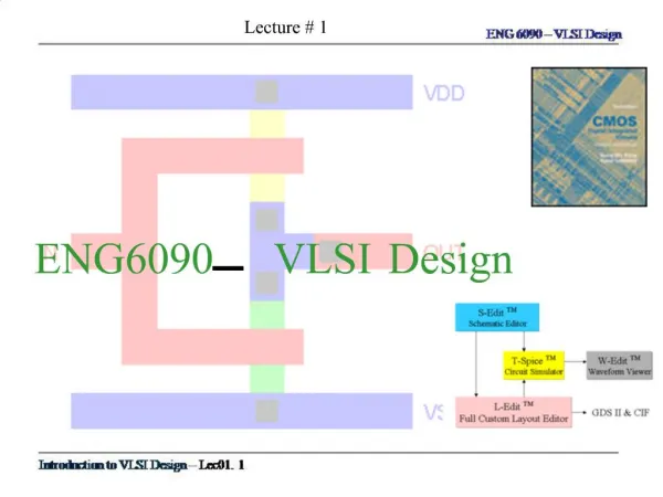
7. Fabrication: After layout and verification, the design is ready for fabrication. Since layout data is typically sent to fabrication on a tape, the event of release of data is called Tape Out.Layout data is converted (or fractured) into photo-lithographic masks, one for each layer. Masks identify spaces on the wafer, where certain materials need to be deposited, diffused or even removed. Silicon crystals are grown and sliced to produce wafers. Extremely small dimensions of VLSI devices require that the wafers be polished to near perfection. The fabrication process consists of several steps involving deposition, and diffusion of various materials on the wafer. During each step one mask is used. Several dozen masks may be used to complete the fabrication process. A large wafer is 20 cm (8 inch) in diameter and can be used to produce hundreds of chips, depending of the size of the chip. Before the chip is mass produced, a prototype is made and tested. Industry is rapidly moving towards a 30 cm (12 inch) wafer allowing even more chips per wafer leading to lower cost per chip. 8. Packaging, Testing and Debugging: Finally, the wafer is fabricated and diced into individual chips in a fabrication facility. Each chip is then packaged and tested to ensure that it meets all the design specifications and that it functions properly. Chips used in Printed Circuit Boards (PCBs) are packaged in Dual In-line Package (DIP), Pin Grid Array (PGA), Ball Grid Array (BGA), and Quad Flat Package (QFP). Chips used in Multi-Chip Modules (MCM) are not packaged, since MCMs use bare or naked chips. Mos Layers: N-diffusion P-diffusion Polysilicon Metal These layers are isolated by one another by thick or thin silicon dioxide insulating layers. Thin oxide mask region includes n-diffusion / p-diffusion and transistor channel. Stick Diagrams: Stick diagrams may be used to convey layer information through use of a color code. For example: n-diffusion -- green poly – red blue -- metal yellow --implant black – contact areas
2Encodings For Nmos Process: Figure shows the way of representing different layers in stick diagram notation and mask layout using nmos style. Figure1 shows when a n-transistor is formed: a transistor is formed when a green line (n+ diffusion) crosses a red line (poly) completely. Figure also shows how a depletion mode transistor is represented in the stick format.
Encodings for CMOS process: Figure 2 shows when a n-transistor is formed: a transistor is formed when a green line (n+ diffusion) crosses a red line (poly) completely. Figure 2 also shows when a p-transistor is formed: a transistor is formed when a yellow line(p+ diffusion) crosses a red line (poly) completely.
Encoding for BJT and MOSFETs: There are several layers in an nMOS chip: a p-type substrate paths of n-type diffusion a thin layer of silicon dioxide paths of polycrystalline silicon a thick layer of silicon dioxide paths of metal (usually aluminium) a further thick layer of silicon dioxide with contact cuts through the silicon dioxide where connections are required. The three layers carrying paths can be considered as independent conductors that only interact where polysilicon crosses diffusion to form a transistor. These tracks can be drawn as stick diagrams wih
diffusion in green polysilicon in red metal in blue using black to indicate contacts between layers and yellow to mark regions of implant in the channels of depletion mode transistors. With CMOS there are two types of diffusion: n-type is drawn in green and p-type in brown. These are on the same layers in the chip and must not meet. In fact, the method of fabrication required that they be kept relatively far apart.Modern CMOS processes usually support more than one layer of metal. Two are common and three or more are often available. Actually, these conventions for colors are not universal; in particular, industrial (rather than academic) systems tend to use red for diffusion and green for polysilicon. Morever shortage of colored pen normally mean that both types of diffusion in CMOS are colored green and the polarity indicated by drawing a circle round by p-type transistor or from the context. Colorings for multiple layers of metal are even less standard. There are three ways that nMOS inverter might be drawn: Figure 4 shows schematic, stick diagram and corresponding layout of nMOS depletion load inverter
Figure 5 shows schematic, stick diagram and corresponding layout of CMOS inverter
Figure 7 shows the stick diagram nMOS implementation of the function f=[(xy)+z]’ Figure 8: stick diagram of CMOS NAND and NOR Figure 8 shows the stick diagram CMOS NOR and NAND, where we can see that the p diffusion line never touched the n diffusion directly, it is always joined using a blue color metal line. NMOS and CMOS Design style: In the NMOS style of representing the sticks for the circuit, we use only NMOS transistor, in CMOS we need to differentiate n and p transistor, that is usually by the color or in monochrome diagrams we will have a demarcation line. Above the demarcation line are the p transistors and below the demarcation are the n transistors. Following stick shows CMOS circuit example in monochrome where we utilize the demarcation line.
Figure 9 shows the stick diagram of dynamic shift register using CMOS style. Here the output of the TG is connected as the input to the inverter and the same chain continues depending the number of bits. Design Rules: Design rules include width rules and spacing rules. Mead and Conway developed a set of simplified scalable λ -based design rules, which are valid for a range of fabrication technologies. In these rules, the minimum feature size of a technology is characterized as 2λ . All width and spacing rules are specified in terms of the parameter λ . Suppose we have design rules that call for a minimum width of 2λ , and a minimum spacing of 3λ. If we select a 2µm technology (i.e., λ = 1 um), the above rules translated to a minimum width of 2µm and a minimum spacing of 3 µm. On the otherhand, if a 1µm technology (i.e., λ = 0.5 µm) is selected, then the same width and spacing rules are now specified as 1 um and 1.5 µm, respectively. Figure 10 shows the design rule n diffusion, p diffusion, poly, metal1 and metal 2. The n and p diffusion lines is having a minimum width of 2λand a minimum spacing of 3λ. Similarly we are showing for other layers.
Figure shows the design rule for the transistor, and it also shows that the poly should extend for a minimum of 2λbeyond the diffusion boundaries.(gate over hang distance) Via: It is used to connect higher level metals from metal1 connection. The cross section and layout view given figure13 explain via in a betterway.
The above figure shows the design rules for contact cuts and Vias. The design rule for contact is minimum 2λx2λand same is applicable for a Via. Buried contact: The contact cut is made down each layer to be joined and it is shown in figure 14 . Butting contact: The layers are butted together in such a way the two contact cuts become contiguous. We can better under the buttingcontact from figure 15
CMOS LAMBDA BASED DESIGN RULES: Till now we have studied the design rules wrt only NMOS , what are the rules to be followed if we have the both p and n transistor on the same chip will be made clear with the diagram. Figure 16 shows the rules to be followed in CMOS well processes to accommodate both n and p transistors. Orbit 2µm CMOS process: In this process all the spacing between each layersand dimensions will be in terms micrometer. The 2µm here represents the feature size. All the design rules what ever we have seen will not have lambda instead it will have the actual dimension in micrometer. In one way lambda based design rules are better compared micrometer based design rules, that is lambda based rules are feature size independent. Figure 17 shows the design rule for BiCMOS process using orbit 2um process.
The following is the example stick and layout for 2way selector with enable (2:1 MUX).
Layout diagram of cmos inverter: In the following, the mask layout design of a CMOS inverter will be examined step- by-step. The circuit consists of one nMOS and one pMOS transistor, therefore, one would assume that the layout topology is relatively simple. Yet, we will see that there exist quite a number of different design possibilities even for this very simple circuit. First, we need to create the individual transistors according to the design rules. Assume that we attempt to design the inverter with minimum-size transistors. The width of the active area is then determined by the minimum diffusion contact size (which is necessary for source and drain connections) and the minimum separation from diffusion contact to both active area edges. The width of the polysilicon line over the active area (which is the gate of the transistor) is typically taken as the minimum poly width . Then, the overall length of the active area is simply determined by the following sum: (minimum poly width) + 2 x (minimum poly-to- contact spacing) + 2 x (minimum spacing from contact to active area edge). The pMOS transistor must be placed in an n-well region, and the minimum size of the n- well is dictated by the pMOS active area and the minimum n-well overlap over n+. The distance between the nMOS and the pMOS transistor is determined by the minimum separation between the n+ active area and the n-well. The polysilicon gates of the nMOS and the pMOS transistors are usually aligned. The final step in the mask layout is the local interconnections in metal, for the output node and for the VDD and GND contacts. Notice that in order to be biased properly, the n-well region must also have a VDD contact. Dimensions of minimum size transistor
Placement of nmos and pmos transistors Layout of cmos inverter
Layout of CMOS NAND and NOR Gates: The mask layout designs of CMOS NAND and NOR gates follow the general principles examined earlier for the CMOS inverter layout. Figure 18 shows the sample layouts of a two- input NOR gate and a two-input NAND gate, using single-layer polysilicon and single-layer metal. Here, the p-type diffusion area for the pMOS transistors and the n- type diffusion area for the nMOS transistors are aligned in parallel to allow simple routing of the gate signals with two parallel polysilicon lines running vertically. Also notice that the two mask layouts show a very strong symmetry, due to the fact that the NAND and the NOR gate are have a symmetrical circuit topology. Finally, Figs 19 and 20 show the major steps of the mask layout design for both gates, starting from the stick diagram and progressively defining the mask layers. Figure 18: Sample layouts of a CMOS NOR2 gate and a CMOS NAND2 gate.
Figure 19: Major steps required for generating the mask layout of a CMOS NOR2 gate.
Figure 20: Major steps required for generating the mask layout of a CMOS NAND2 gate.
Scaling of MOS Circuits: 1.What is Scaling? Proportional Adjustment of the dimensions of an electronic device while maintaining the electrical Properties of the device, results in a device either larger or smallerthan the un-scaled device. Then Which way do we scale the devices for VLSI?BIG and SLOW … or SMALLand FAST? What do we gain? 2.Why Scaling?... Scale the devices and wires down, Make the chips ‘fatter’ – functionality, intelligence, memory – and – faster, Make more chips per wafer – increased yield, Make the end user Happy by giving more for less and therefore, make MORE MONEY!! 3.FoM for Scaling Impact of scaling is characterized in terms of several indicators: Minimum feature size Number of gates on one chip Power dissipation Maximum operational frequency Die size Production cost Many of the FoMs can be improved by shrinking the dimensions of transistors and interconnections. Shrinking the separation between features – transistors and wires Adjusting doping levels and supply voltages. Technology Scaling : Goals of scaling the dimensions by 30%: Reduce gate delay by 30% (increase operating frequency by 43%) Double transistor density Reduce energy per transition by 65% (50% power savings @ 43% increase in frequency) Die size used to increase by 14% per generation Technology generation spans 2-3 years Figure1 to Figure 5 illustrates the technology scaling in terms of minimum feature size, transistor count, prapogation delay, power dissipation and density and technology generations.