Non-MOSFET Based Memory
Non-MOSFET Based Memory. Alex Rodriguez-Triana Terence Frederick April 21, 2008. Outline. MOSFET Based RAM Memory DRAM, SRAM, FLASH Problems with MOSFET Memory Scaling Alternative Memory MRAM FeRAM PCRAM Summary. History of MOSFET Memory. Concept goes back to the 1960s

Non-MOSFET Based Memory
E N D
Presentation Transcript
Non-MOSFET Based Memory Alex Rodriguez-Triana Terence Frederick April 21, 2008
Outline • MOSFET Based RAM Memory • DRAM, SRAM, FLASH • Problems with MOSFET Memory • Scaling • Alternative Memory • MRAM • FeRAM • PCRAM • Summary
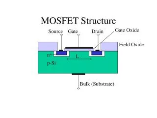
History of MOSFET Memory • Concept goes back to the 1960s • People were speculative • BJT was more advanced and faster • Leakage current • They were attractive • Simple Processing • Layout Advantages • Leads to high-density integrated circuits
History of MOSFET Memory • SRAM were proposed • six MOSFET’s per cell • SRAM began to be used in the mid-70s • DRAM patented in 1968 • 1 MOSFET, 1 Capacitor • First commercial DRAM • 1971 by Intel
Dynamic RAM • Most common type of RAM memory • Arranged in a square array • one capacitor and transistor per cell • Stores one bit per cell • Recharging/Refreshing : capacitors lose their charge • Rows: Word Lines • Columns: Bit Lines
Advantages/Disadvantages of DRAM • Advantages • Cost • Small • 1T & 1C vs. 6T for SRAM • Number of Read/Write Cycles • > 10^15 • Disadvantages • Slow • Need to refresh • Volatile • Data is lost when memory is not powered
Static RAM • Memory cell uses flip-flop to store bit • Requires 6 transistors • Each bit is stored on 4 transistors that form two inverters • Two other transistors control the access to a cell during read and write operations • This storage cell has two stable states • 0 and 1
Advantages/Disadvantages of SRAM • Advantages • Performance better than DRAM • Faster • Less Power Hungry • Number of Read/Write Cycles • > 10^15 • Disadvantages • Cost • More than DRAM • Volatile • Data is lost when memory is not powered
FLASH Memory • Invented by Dr. Fujio Masuoka at Toshiba in 1984 • Stores information in an array of memory cells made from floating-gate transistors • Single-Level Cell Devices - each cell stores only one bit
Advantages/Disadvantages of FLASH • Advantages • Cost • Non-Volatile • Does not lose information when the power is off • Low Power • Fast Erase • Large blocks rather than one word at a time • Disadvantages • Number of Read/Write Cycles • ~ 10^6 • Slow Write • Entire block must be read, word updated, then entire block written back
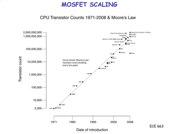
Future of MOSFET Memory • Current memory technologies are nearing the end • Main issue with MOSFET RAMs • Scalability • Designers put more components onto each chip • Width of the smallest features is shrinking • 130 nm in 2000 to 45 nm today • Existing memory technologies will be good for several more generations • Unlikely to make the transition to 22 nm (scheduled for 2011) or 16 nm (2018) • New types of technologies • MRAM, FeRAM, PCRAM
MOSFET Scaling • Late 1990s • Scaling resulted in great improvement in MOSFET circuit operation • Reasons for smaller MOSFETs • Same functionality in a smaller area • Reduces cost per chip • Smaller ICs allow for more chips on a wafer • Fab costs for wafer are relatively fixed
MOSFET Scaling • Problems when scaling too small • Slower chip speed • Greater delay due to interconnects • Operational problems • Higher sub-threshold, increased gate-oxide and junction leakage, lower transconductance, heat production, and process variation • Simulation • Difficult to predict what the final device will look like • Modeling of physical processes • Microscopic variations in structure due to the probabilistic nature of atomic processes require statistical predictions
Alternative Technologies • Magnetic RAM (MRAM) • Ferroelectric RAM (FeRAM) • Phase Change RAM (PCRAM)
Magnetoresistive RAM • Under development since the 1990s • Data is stored by magnetic storage elements • Formed from two ferromagnetic plates • Plates can hold a magnetic field • Polarization doesn’t leak away with time like charge • Less wear since switching states doesn’t involve movement of electron or atoms • One plates is a permanent magnet • Set to a certain polarity • Second plate’s field will change to match that of an external field • A memory device is built from a grid of "cells"
4MB MRAM • 1st commercial available MRAM • Based on 1T and 1 magnetic tunnel junction • Isolates read and write path • Separates programming components from the sense circuit • Improved performance
Read and Write of MRAM • Read • Current is passedthrough the bit • resistance of thebit is sensed • Write • Current is passed through the programming lines • Induced magnetic field is created at the junction, which the writable plate picks up
MRAM • Cell works in a toggling mode • Same direction • Low resistance state (0) • Opposite direction • High resistance state (1)
MRAM in Embedded Systems • Inserted late in the SC fabrication process • Low temperature • Compatible with CMOS processing • Consolidate multiple MRAM into one • highly reliable NVRAM • Less complexity • High performance RD/WR
Advantages/Disadvantages of MRAM • Advantages • Non-volatile • Does not require programming sequences or block erasing • Very fast RD/WR and unlimited endurance • Simple device Architecture and easy software development • Due to easy write and overwrite • Disadvantages • Scalability of magnetic domain? • Might have the same problems as a transistor • Disturbance of neighboring cells when put close together • Leads to false writes • High power needed to write
Ferroelectric RAM Borrows concepts from DRAM most popular design follows the 1T1C design concept similar/same write process write accomplished by applying charge that is stored in capacitor Similarity to Floating Gate Design 1T design Also reminiscent of MRAM focuses on ferroelectric properties, whereas MRAM techniques often focus on ferromagnetic properties both characteristics take form of hysteresis loop
Structure 1T type Similar to normal transistor Identical to floating gate design where floating gate is ferroelectric material 1T1C type ferroelectric material serves ONLY as capacitor
“Recent Progress in Ferroelectric Memory Technology” by Hiroshi Ishiwara
Introduction Two major focuses in the paper developing a better material to deal with leakage currents in 1T1C FeRAM replace some Fe in lattice with Mn Improve upon 1T FeRAM design create MFIS-FET Introduce a new 1T2C FeRAM design
1T2C Design 2 Ferroelectric capacitors of the same size connected to the gate of the transistor capacitors polarized opposite the gate Good performance non-destructive data reads good data retention time high on/off current ratio
Advantages/Disadvantages of FeRAM Advantages lower power usage faster write speed greater number of rewrites already being mass-produced Disadvantages still more research to be done on reliability (i.e. high NRE cost) only applicable to a small niche
“Study of Phase Change Random Access Memory (PCRAM) at the Nano-Scale” by R. Zhao, L.P. Shi, W.J. Wang, H.X. Yang, H.K. Lee, K.G. Lim, E.G. Yeo, E.K. Chua and T.C. Chong
Introduction RAM based on floating-gate design (i.e. Flash memory) will soon meet physical limitations interpoly tunneling intercell crosstalk Flash memory is the most prevalent non-volatile memory on the market a viable option must be found soon PCRAM may be that option
Fabrication/Design “Bybrid” process used to etch the layers Electronic Beam Lithography (EBL) Optical Lithography Electrodes made of TiW Dielectric is common SiO2 Phase Change material is Ge2Sb5Te2 Feature size refers to contact between PC and bottom electrode
How it Works Unique Phase Change material has two states Crystalline state has low resistance and represents a stored ‘1’ Amorphous state has high resistance and represents a stored ‘0’ To change bit from 1 to 0 (i.e. RESET), a relatively high voltage is applied for a short time such that the compound melts but is not able to recrystallize To change bit from 0 to 1 (i.e. SET), a lower voltage is applied for a longer time so that compound can crystallize
Simulation Pulse generator created to produce short (<10ns) signal Known resistance placed in circuit Voltages measured to determine drop across resistor Current into PCRAM approximately (V1-V2)/Rload Cells with feature sizes ranging from 40 to 200 nm created same wafer used
Advantages/Disadvantages of PCRAM Advantages great scalability fast for both reads and writes low current required to program Disadvantages as of yet, only in the research phase still limited read/write accesses (108)